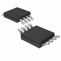
LTC4357CMS8#TRPBF Linear Technology, LTC4357CMS8#TRPBF Datasheet - Page 3

LTC4357CMS8#TRPBF
Manufacturer Part Number
LTC4357CMS8#TRPBF
Description
IC IDEAL DIODE CNTRLR 8-MSOP
Manufacturer
Linear Technology
Datasheet
1.LTC4357CDCBTRMPBF.pdf
(14 pages)
Specifications of LTC4357CMS8#TRPBF
Applications
Redundant Power Supplies, Telecom Infrastructure
Fet Type
N-Channel
Number Of Outputs
1
Internal Switch(s)
No
Delay Time - Off
300ns
Voltage - Supply
9 V ~ 80 V
Current - Supply
500µA
Operating Temperature
0°C ~ 70°C
Mounting Type
Surface Mount
Package / Case
8-MSOP, Micro8™, 8-uMAX, 8-uSOP,
Lead Free Status / RoHS Status
Lead free / RoHS Compliant
Delay Time - On
-
Available stocks
Company
Part Number
Manufacturer
Quantity
Price
electrical characteristics
temperature range, otherwise specifications are at T
Note 1: Stresses beyond those listed under Absolute Maximum Ratings
may cause permanent damage to the device. Exposure to any Absolute
Maximum Rating condition for extended periods may affect device
reliability and lifetime.
typical perForMance characteristics
SYMBOL
V
I
I
I
DV
I
I
t
DV
DD
IN
OUT
GATE(UP)
GATE(DOWN)
OFF
DD
GATE
SD
200
800
600
400
0
V
0
DD
V
DD
Current (I
= V
OUT
20
= V
PARAMETER
Operating Supply Range
Supply Current
IN Pin Current
OUT Pin Current
External N-Channel Gate Drive
(V
External N-Channel Gate Pull-Up Current V
External N-Channel Gate Pull-Down
Current in Fault Condition
Gate Turn-Off Time
Source-Drain Regulation Voltage
(V
IN
GATE
IN
DD
± 1V
V
– V
DD
40
vs V
– V
(V)
OUT
IN
DD
)
)
)
60
4357 G01
80
400
300
200
100
0
A
0
IN Current (I
= 25°C. V
V
DD
CONDITIONS
V
V
V
V
V
V
V
V
IN
IN
DD
DD
GATE
GATE
IN
GATE
GATE
= V
The
= V
= V
, V
, V
– V
OUT
20
= V
= V
– V
– V
OUT
OUT
OUT
OUT
OUT
= V
l
OUT
IN
IN
IN
IN
denotes the specifications which apply over the full operating
= 20V to 80V
= 9V to 20V
IN
IN
±1V
±1V
= 55mV
, V
V
+ 5V
< 1V, C
= 2.5V
+ 1V
DD
= V
vs V
V
IN
IN
40
= V
Note 2: All currents into pins are positive, all voltages are referenced to
GND unless otherwise specified.
Note 3: An internal clamp limits the GATE pin to a minimum of 10V above
IN or 100V above GND. Driving this pin to voltages beyond this clamp may
damage the device.
– V
(V)
DD
IN
OUT
GATE
–
, V
OUT
|
)
–
–1V,
= V
DD
= 0pF
= 0.1V
IN
60
= 9V to 80V unless otherwise noted.
– 1V
4357 G02
80
180
150
120
l
l
l
l
l
l
l
l
l
l
90
60
30
0
0
OUT Current (I
MIN
150
–14
4.5
10
10
9
1
V
V
DD
DD
20
= V
= V
OUT
OUT
TYP
350
–20
300
0.5
80
12
25
6
2
= V
V
= V
OUT
OUT
40
LTC4357
IN
IN
(V)
+ 1V
vs V
– 1V
MAX
1.25
500
210
–26
500
80
15
15
55
OUT
60
)
UNITS
4357 G03
4357fd
mA
mV
80
µA
µA
µA
ns
V
V
V
A


