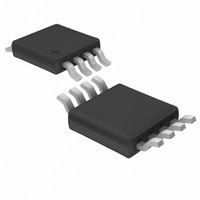
LTC4357CMS8#TRPBF Linear Technology, LTC4357CMS8#TRPBF Datasheet - Page 8

LTC4357CMS8#TRPBF
Manufacturer Part Number
LTC4357CMS8#TRPBF
Description
IC IDEAL DIODE CNTRLR 8-MSOP
Manufacturer
Linear Technology
Datasheet
1.LTC4357CDCBTRMPBF.pdf
(14 pages)
Specifications of LTC4357CMS8#TRPBF
Applications
Redundant Power Supplies, Telecom Infrastructure
Fet Type
N-Channel
Number Of Outputs
1
Internal Switch(s)
No
Delay Time - Off
300ns
Voltage - Supply
9 V ~ 80 V
Current - Supply
500µA
Operating Temperature
0°C ~ 70°C
Mounting Type
Surface Mount
Package / Case
8-MSOP, Micro8™, 8-uMAX, 8-uSOP,
Lead Free Status / RoHS Status
Lead free / RoHS Compliant
Delay Time - On
-
Available stocks
Company
Part Number
Manufacturer
Quantity
Price
LTC4357
applications inForMation
Design Example
The following design example demonstrates the calcula-
tions involved for selecting components in a 12V system
with 10A maximum load current (see Figure 4).
First, calculate the R
sired forward drop at full load. Assuming V
The Si4874DY offers a good solution, in an S8 package
with R
The maximum power dissipation in the MOSFET is:
With less than 39µF of local bypass, the recommended RC
values of 100Ω and 0.1µF were used in Figure 4.
Since BV
ing is unnecessary.
P = I
R
R
DS(ON)
DS(ON)
DS(ON)
LOAD
DSS
≤
≤ 10mΩ
2
+ V
= 10mΩ(max) and BV
V
• R
I
LOAD
DROP
V
IN
IN
DS(ON)
is much less than 100V, output clamp-
DS(ON)
INPUT PARASITIC
=
INDUCTANCE
+
INPUT
SHORT
V
IN
0.1V
10A
= (10A)
Figure 2. Reverse Recovery Produces Inductive Spikes at the IN and OUT Pin.
The Polarity of Step Recovery Spikes is Shown Across Parasitic Inductances
of the MOSFET to achieve the de-
Figure 3. Protecting Against Collapse of V
–
INPUT
SHORT
2
D
SBR1U-
150SA
IN
• 10mΩ = 1W
DSS
IN
IN
of 30V.
REVERSE RECOVERY CURRENT
DROP
LTC4357
GATE
GND
M1
LTC4357
= 0.1V,
GATE
GND
M1
OUT
V
4357 F03
DD
OUT
V
4357 F02
DD
V
V
12V
12V
DD
IN1
IN2
R1
100
C1
100nF
During Reverse Recovery
OR
C
10µF
OUTPUT PARASITIC
OUT
IN
IN
INDUCTANCE
Figure 4. 12V, 10A Diode-OR
C
OR
OUT
OUTPUT PARASITIC
Si4874DY
Si4874DY
LTC4357
LTC4357
D
SMAT70A
INDUCTANCE
+
GATE
GATE
GND
GND
M1
M2
CLAMP
C
LOAD
V
OUT
–
OUT
OUT
4357 F04
V
V
DD
DD
C
V
LOAD
OUT
R1
100
R1
100
C1
0.1µF
C1
0.1µF
V
TO LOAD
OUT
4357fd


