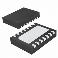
LTC4355CDE#TRPBF Linear Technology, LTC4355CDE#TRPBF Datasheet - Page 8

LTC4355CDE#TRPBF
Manufacturer Part Number
LTC4355CDE#TRPBF
Description
IC IDEAL DIODE-OR 14-DFN
Manufacturer
Linear Technology
Datasheet
1.LTC4355ISPBF.pdf
(20 pages)
Specifications of LTC4355CDE#TRPBF
Applications
-48V Dist Power Systems, AdvancedTCA ® Systems
Fet Type
N-Channel
Number Of Outputs
2
Internal Switch(s)
No
Delay Time - Off
300ns
Voltage - Supply
9 V ~ 80 V
Current - Supply
2mA
Operating Temperature
0°C ~ 70°C
Mounting Type
Surface Mount
Package / Case
14-DFN
Lead Free Status / RoHS Status
Lead free / RoHS Compliant
Delay Time - On
-
Available stocks
Company
Part Number
Manufacturer
Quantity
Price
APPLICATIONS INFORMATION
LTC4355
MOSFET Selection
The LTC4355 drives N-channel MOSFETs to conduct the
load current. The important features of the MOSFETs are
on-resistance R
V
The gate drive for the MOSFET is guaranteed to be greater
than 4.5V when the supply voltage at V
9V and 20V. When the supply voltage at V
than 20V, the gate drive is guaranteed to be greater than
10V. The gate drive is limited to less than 18V. This allows
the use of logic level threshold N-channel MOSFETs and
standard N-channel MOSFETs above 20V. An external
Zener diode can be used to clamp the potential from the
MOSFET’s gate to source if the rated breakdown voltage
is less than 18V. See the Typical Applications section for
an example.
The maximum allowable drain-source voltage, BV
must be higher than the supply voltages. If an input is
connected to GND, the full supply voltage will appear
across the MOSFET.
If the voltage drop across either MOSFET exceeds the con-
fi gurable ΔV
PWRFLT pin corresponding to the faulting channel pull low.
The R
load current while not triggering a fault, and to stay within
the MOSFET’s power rating at the maximum load current
(I
Fault Conditions
The LTC4355 monitors fault conditions and shunts current
away from LEDs or opto-couplers, turning each one off to
indicate a specifi c fault condition (see Table 1).
When the voltage drop across the pass transistor is
higher than the confi gurable ΔV
internal pull-down at the VDSFLT pin and the PWRFLT1 or
PWRFLT2 pin corresponding to the faulting channel turns
on. The ΔV
Tying SET to GND, tying SET to a 100k resistor connected
to GND, or fl oating SET confi gures ΔV
500mV, or 1.5V respectively.
8
DSS
2
• R
, and the threshold voltage.
DS(ON)
DS(ON)
SD(FLT)
should be small enough to conduct the maximum
SD(FLT)
).
DS(ON)
threshold is confi gured by the SET pin.
fault threshold, the VDSFLT pin and the
, the maximum drain-source voltage
SD(FLT)
fault threshold, the
SD(FLT)
OUT
OUT
is between
to 250mV,
is greater
DSS
,
Fault conditions that may cause a high voltage across the
pass transistor include: a MOSFET open on the higher
supply, excessive MOSFET current due to overcurrent
on the load or a shorted MOSFET on the lower supply.
During startup or when a switchover between supplies
occurs, the VDSFLT pin and PWRFLT1 or PWRFLT2 pin
may momentarily indicate that the forward voltage has
exceeded the programmed threshold during the short
interval when the MOSFET gate ramps up and the body
diode conducts.
The PWRFLT pins are additionally used to indicate if either
input supply is below its normal regulation range. If the
voltage at the MON1 or MON2 pin is less than V
typically 1.23V, the corresponding PWRFLT1 or PWRFLT2
pin will pull low. A resistive divider connected to the input
supply drives the MON pin for the corresponding supply,
confi guring the PWRFLT threshold for that supply. Be sure
to account for the tolerance of the MON pin threshold,
the resistor tolerances, and the regulation range of the
supply being monitored. Also, ensure that the voltage on
the MON pin will not exceed 7V.
The FUSEFLT pins are used to indicate the status of the
input fuses. If one of the IN pins falls below V
cally 3.5V, the FUSEFLT pin corresponding to that supply
will pull low. The IN pins each sink a minimum of 0.5mA,
enough to pull the pin low after an input fuse blows open.
If there is a possibility that the MOSFET leakage current
can be greater than 0.5mA, a resistor can be connected
between the IN pin and GND to sink more current. Note
that if the input supply voltage is less than V
FUSEFLT pin will pull low.
Table 1. Fault Table
< ΔV
*ΔV
ΔV
False
False
False
False
True
True
True
True
SD2
SD(FLT)
SD1
< ΔV
SD(FLT)
> 3.5V
False
False
False
False
V
True
True
True
True
IN1
> 1.23V
V
False
False
False
False
True
True
True
True
MON1
Pull-Down
Pull-Down
Pull-Down
Pull-Down
VDSFLT*
Hi-Z
Hi-Z
Hi-Z
Hi-Z
Pull-Down
Pull-Down
Pull-Down
Pull-Down
FUSEFLT1
Hi-Z
Hi-Z
Hi-Z
Hi-Z
INx(TH)
INx(TH)
Pull-Down
Pull-Down
Pull-Down
Pull-Down
Pull-Down
Pull-Down
PWRFLT1
MON(TH)
Hi-Z
Hi-Z
, typi-
4355fe
the
,


