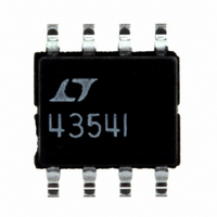
LTC4354IS8#PBF Linear Technology, LTC4354IS8#PBF Datasheet - Page 9

LTC4354IS8#PBF
Manufacturer Part Number
LTC4354IS8#PBF
Description
IC MON DIODE-OR CTLR NEG 8SOIC
Manufacturer
Linear Technology
Datasheet
1.LTC4354CS8PBF.pdf
(12 pages)
Specifications of LTC4354IS8#PBF
Applications
-48V Dist Power Systems, AdvancedTCA ® Systems
Fet Type
N-Channel
Number Of Outputs
2
Internal Switch(s)
No
Delay Time - Off
700ns
Voltage - Supply
4.5 V ~ 11.75 V
Current - Supply
1.2mA
Operating Temperature
-40°C ~ 85°C
Mounting Type
Surface Mount
Package / Case
8-SOIC (3.9mm Width)
Lead Free Status / RoHS Status
Lead free / RoHS Compliant
Delay Time - On
-
Available stocks
Company
Part Number
Manufacturer
Quantity
Price
APPLICATIO S I FOR ATIO
The worst case power dissipation in R
Choose a 12k 0.5W resistor or use two 5.6k 0.25W
resistors in series.
Next, choose the N-channel MOSFET. The 100V, IRF3710S
in D
good solution. The maximum voltage drop across it is:
The maximum power dissipation in the FET is a mere:
R1 and R2 are chosen to be 2k to protect DA and DB pins
from being damaged by high voltage spikes that can occur
during an input supply fault.
V
V
A
B
= –5.2V
= –5.2V
∆V = (5A)(23mΩ) = 115mV
P = (5A)(115mV) = 0.6W
P
2
GND
=
Pak package with R
(
72
V
−
12
DA
10 5
1
k
–5.2V Diode-Or Controller
.
DB
8
U
V
)
2
Si4466DY
=
M1
GA
LTC4354
DS(ON)
U
V
4
0 315
CC
.
3
Si4466DY
W
= 23mΩ (max.) offers a
GB
M2
6
W
FAULT
IN
V
SS
:
2, 5
1µF
C
IN
7
U
D1
LED
R3
2k
4354 TA02
LOAD
The LED, D1, requires at least 1mA of current to fully turn
on, therefore R3 is set to 33k to accommodate lowest input
supply voltage of –36V.
Layout Considerations
The following advice should be considered when laying
out a printed circuit board for the LTC4354.
The bypass capacitor provides AC current to the device so
place it as close to the V
inputs to the servo amplifiers, DA, DB and V
be connected directly to the MOSFETs’ terminals using
Kelvin connections for good accuracy.
Keep the traces to the MOSFETs wide and short. The PCB
traces associated with the power path through the MOSFETs
should have low resistance.
Positive Low Voltage Diode-OR Combines
INPUT
INPUT
1µF
1µF
100A
100A
1.2V
1.2V
Multiple Switching Converters
240Ω*
240Ω*
V
V
EE
EE
*OPTIONAL PRELOAD
HAT2165 ×6
HAT2165 ×6
CC
LTC4354
LTC4354
GA,GB
GA,GB
12V
V
12V
V
and V
CC
CC
470Ω
470Ω
DA,DB
DA,DB
SS
pins as possible. The
4354 TA02b
LTC4354
SS
1.2V, 200A
OUTPUT BUS
pins, should
4354fb
9


