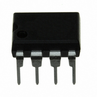
LX1562IM Microsemi Analog Mixed Signal Group, LX1562IM Datasheet - Page 5

LX1562IM
Manufacturer Part Number
LX1562IM
Description
IC PFC CONTROLLER 8DIP
Manufacturer
Microsemi Analog Mixed Signal Group
Datasheet
1.LX1562IM.pdf
(25 pages)
Specifications of LX1562IM
Mode
Discontinuous Conduction (DCM)
Frequency - Switching
1.7MHz
Current - Startup
200µA
Voltage - Supply
11 V ~ 25 V
Operating Temperature
0°C ~ 100°C
Mounting Type
Through Hole
Package / Case
8-DIP
Lead Free Status / RoHS Status
Contains lead / RoHS non-compliant
Available stocks
Company
Part Number
Manufacturer
Quantity
Price
Company:
Part Number:
LX1562IM
Manufacturer:
LINFINEONINI
Quantity:
5 510
Company:
Part Number:
LX1562IM
Manufacturer:
SIEMENS
Quantity:
5 510
Part Number:
LX1562IM
Manufacturer:
LINFINTY
Quantity:
20 000
Copyright © 1996
Rev. 1.3a
FUNCTIONAL DESCRIPTION
E.A. OUT
MULT IN
GND
OUT
C.S.
Pin
INV
V
I
L1
DET
IN
8/30
L1
MULT
# Description
8
6
1
2
3
4
5
7
V
IN
I
DET
8
3
5
IN
300
Input supply voltage.
Input supply voltage return. Must always be the lowest potential of all the pins.
Inverting input of the Error Amplifier. The output of the Boost converter should be resistively divided to 2.5V and
connected to this pin.
The output of the Error Amplifier. A feedback compensation network is placed between this pin and the INV pin.
Input to the multiplier stage. The full-wave rectified AC is divided to less than 2V and is connected to this pin.
Input to the PWM comparator. Current is sensed in the Boost stage MOSFET by a resistor in the source lead, and is
fed to this pin. An internal blanking circuit eliminates the RC low pass filter that otherwise is required to eliminate leading
edge spike.
A current driven logic input with internal clamp.
A second winding on the Boost inductor senses the flyback voltage associated with the zero crossing of the inductor
current and feeds it to the I
PWM output pin. A totem-pole output stage specially designed for direct driving the MOSFET.
13.1V (1562)
9.8V (1563)
1.72V
5.2V (1562)
2.1V (1563)
P R O D U C T D A T A B O O K 1 9 9 6 / 1 9 9 7
B L O C K D I A G R A M / P I N D E S C R I P T I O N S
S
E C O N D
V
REF
P
DET
V
-G
R O D U C T I O N
TIMER
pin through a limiting resistor. Low on this pin causes V
UVLO
E N E R AT I O N
Internal
Bias
R
Internal Circuitry
S
6.8V To All
Delay
1µs
LATCH
P
O W E R
2.5V
REF
D
Q
A T A
F
1.24V
Q
C.S.
A C T O R
M1
V
REF
S
C
H E E T
O N T R O L L E R
M2
Input
1.8V
AC
Filter
EMI
O
LX1562/1563
(pin 7) to go high.
C.S.
V
REF
E.A. INV.
E.A. OUT
OUT
C.S.
1
2
7
4
V
IN
C1
L1
D1
5


