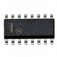
NCP1651DR2G ON Semiconductor, NCP1651DR2G Datasheet - Page 19

NCP1651DR2G
Manufacturer Part Number
NCP1651DR2G
Description
IC PFC CONTROLLER CCM/DCM 16SOIC
Manufacturer
ON Semiconductor
Datasheet
1.NCP1651DR2G.pdf
(32 pages)
Specifications of NCP1651DR2G
Mode
Continuous Conduction (CCM), Discontinuous Conduction (DCM)
Frequency - Switching
250kHz
Current - Startup
8.5mA
Voltage - Supply
10 V ~ 18 V
Operating Temperature
-40°C ~ 125°C
Mounting Type
Surface Mount
Package / Case
16-SOIC (3.9mm Width)
Switching Frequency
25 KHz to 250 KHz
Maximum Operating Temperature
+ 125 C
Mounting Style
SMD/SMT
Minimum Operating Temperature
- 40 C
Lead Free Status / RoHS Status
Lead free / RoHS Compliant
Other names
NCP1651DR2GOS
NCP1651DR2GOS
NCP1651DR2GOSTR
NCP1651DR2GOS
NCP1651DR2GOSTR
Available stocks
Company
Part Number
Manufacturer
Quantity
Price
Part Number:
NCP1651DR2G
Manufacturer:
ON/安森美
Quantity:
20 000
resistor, with a nominal value of 25 kΩ. This is because the
resistor that converts the A input voltage into a current is
internal. Making both of these resistors internal, allows for
good accuracy and good temperature performance. Only a
capacitor needs to added externally to properly compensate
this multiplier. It is not recommended that an external
parallel resistor be used at the “Ref Gain” pin, due to
tolerance variations of the internal resistor.
reference multiplier. It is due to the V- -I converter that feeds
the input.
converter for the appropriate signal into the multiplier. The
schematic for that converter follows.
Error Amplifier for ESD protection. Due to this resistor, the
voltage on pin 10 (AC Ref) will exceed 4.5 volts under some
conditions, but the maximum voltage at the non- -inverting
AC Error Amplifier input will be clamped at 4.5 volts.
AC Ref
FB/SD
The reference multiplier contains an internal loading
There is an offset in the compensation (A- -input) to the
The FB/SD signal is buffered by a voltage- -to- -current
The output current for this stage is:
There is a 1 k resistor between the AC Ref pin and the AC
Figure 34. Reference Multiplier Clamp Circuit
10
8
V
Figure 33. Multiplier V- -I Converter
fb
Multiplier
3.8 k
i mult =
25 k
+
--
1 k
6 (V fb − 1.5 V)
CURRENT
MIRROR
1.5 V
20 k
i
20 k
1
4.5 V
Reference Multiplier
6 X
i
AC Error
Amplifier
mult
i
+
1
--
http://onsemi.com
19
Feedback/Shutdown
function is to port the error signal to the voltage- -to- -current
converter that feeds the reference multiplier. The operating
range for the feedback signal is from 1.0 to 4.0 volts. Below
an input level of 1.5 volts, the PWM duty cycle is reduced
to zero. At 4.0 volts the PWM is operating at its maximum
duty cycle.
comparator that will shutdown the unit if the voltage falls
below 0.60 volts. Under normal operating conditions the
signal at this input will be 1.5 volts or greater, and the
shutdown circuit will be inactive. This circuit is designed
such that a 680 Ohm resistor in series with the optocoupler
will assure that the converter will go to zero duty cycle when
the opto is on full, but will not go low enough to put the unit
into its shutdown mode.
including overvoltage, undervoltage or hot- -swap control.
An external transistor, open collector or open drain gate,
connected to this pin can be used to pull it low, which will
inhibit the operation of the chip, and change the operating
state to a low power standby mode. An example of a
shutdown circuit is shown in Figure 23.
Ramp Compensation
compensation to be adjusted for optimum performance.
Ramp compensation is necessary in a current mode
converter to stabilize the units operation when the duty cycle
is greater than 50%.
several variables, including the boost inductor value, and the
desires of the designer. The value should be based on the
falling di/dt of the inductor current. For a boost inductor with
a variable input voltage, this will vary over the AC input
cycle, and with changes in the input line. A di/dt chart is
included in the design spreadsheet that is available for the
NCP1651.
compensation should equal the falling di/dt at 100% duty
cycle. For optimum line transient response, it should equal
one half of the falling di/dt at 100% duty cycle.
provides a voltage equal to the ramp on the oscillator C
A resistor from this pin to ground, programs a current that
is transformed via a current mirror to the non- -inverting
input of the PWM comparator.
the PWM comparator is the current shunt voltage at pin 5
multiplied by 10, which is the gain of the current amplifier
output that feeds the PWM.
The FB/SD pin is a multiple function pin. Its primary
The signal at this pin is also sensed by an internal
The shutdown function can be used for multiple purposes
The Ramp Compensation pin allows the amount of ramp
The amount of compensation required is dependant on
For optimum load transient performance, the ramp
This pin is a buffered output of the oscillator, which
The ramp voltage due to the inductor di/dt at the input to
T
pin.


