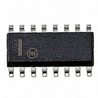
NCP1651DR2G ON Semiconductor, NCP1651DR2G Datasheet - Page 27

NCP1651DR2G
Manufacturer Part Number
NCP1651DR2G
Description
IC PFC CONTROLLER CCM/DCM 16SOIC
Manufacturer
ON Semiconductor
Datasheet
1.NCP1651DR2G.pdf
(32 pages)
Specifications of NCP1651DR2G
Mode
Continuous Conduction (CCM), Discontinuous Conduction (DCM)
Frequency - Switching
250kHz
Current - Startup
8.5mA
Voltage - Supply
10 V ~ 18 V
Operating Temperature
-40°C ~ 125°C
Mounting Type
Surface Mount
Package / Case
16-SOIC (3.9mm Width)
Switching Frequency
25 KHz to 250 KHz
Maximum Operating Temperature
+ 125 C
Mounting Style
SMD/SMT
Minimum Operating Temperature
- 40 C
Lead Free Status / RoHS Status
Lead free / RoHS Compliant
Other names
NCP1651DR2GOS
NCP1651DR2GOS
NCP1651DR2GOSTR
NCP1651DR2GOS
NCP1651DR2GOSTR
Available stocks
Company
Part Number
Manufacturer
Quantity
Price
Part Number:
NCP1651DR2G
Manufacturer:
ON/安森美
Quantity:
20 000
AC Voltage Divider
a simple but important calculation. For this calculation it is
necessary to know the maximum line that the unit can
operate at. The peak input voltage will be:
Vin
(this is true for both multipliers).
voltage is:
resistor (R
power in this resistor is:
PR
so: R
To minimize dissipation, use the next largest standard value,
or 560 kΩ.
Typically, two 1/4 resistors are used in series to handle the
power.
Then, R
Current Sense Resistor/Ramp Compensation
current sense resistor and ramp compensation signal, will
determine the peak instantaneous current that the power
switch will be allowed to conduct before it is turned off.
the signal at the non- -inverting input to the PWM comparator
must add up to 4.0 volts in order to terminate the switch
cycle. These signals are the error signal from the AC error
amp, the ramp compensation signal, and the instantaneous
current. For a worst case condition, the output of the AC
error amp could be zero (current), which would require that
the sum of the ramp compensation signal and current signal
be 4.0 volts. This must be evaluated under full load and low
line conditions.
match the falling di/dt (which has been converted to a dv/dt)
of the inductor at 50% duty cycle. 50% duty cycle will occur
when the input voltage is 50% of the output voltage. Both the
falling di/dt and output voltage need to be reflected by the
transformer turns ratio to the primary side. Thus the
following equations for R
di/dt primary = V
di/dt secondary = V
di/dt reflected to the primary:
The voltage divider from the input rectifiers to ground is
The maximum voltage at the AC input (pin 5) is 3.75 volts
If the maximum line voltage is 265 Vac, the peak input
Vin
To keep the power dissipation reasonable for a 1/2 watt
The combination of the voltage developed across the
The vector sum of the three signals that combine to create
For proper ramp compensation, the ramp signal should
ac1
peak
L S =
V O
ac1
L P
peak
= (375 V - - 3.75 V)
= 1.414 x Vrms
ac2
= 551 kΩ
ac1
= 1.414 x 265 V
N P
N S
N S
N P
= 3.75 V / ((375 V - - 3.75 V) / 560 k) = 5.6 kΩ
), it should dissipate no more than 1/4 watt. The
2
2
⋅ T
L P
in
2
/L
O
⋅
/L
P
N S
N P
T/2
S
max
T/2
2
S
rms
/ R
and R
= 375 V
ac1
RC
= 0.25 watts
must be satisfied:
pk
http://onsemi.com
27
Simplifies to:
V
di/dt primary = di/dt secondary
V
V
Equation 2)
R
di/dt (primary) T R
V
V
R
Equation 3)
t
saturated in a low state, the ramp compensation signal plus
the current signal must equal 4.0 volts (3.8 volts is used to
avoid over driving the amplifier), which is the reference
level for the PWM comparator. So:
Equation 4) Vref
3.8 V = I
Combining equations 2 and 4 gives:
Where:
R
R
t
T is the period for the switching frequency (ms)
L
V
V
P
I
I
V
N
on
on
avg
pk
out
P
out
in
in
S
S
S
RC
rms
O
Rcomp
O
(t)
P
For proper slope compensation, the relationship between
For maximum output current, when the error amplifier is
/N
/L
/L
/L
/L
= T/(N
is the on time for the conditions given (ms)
is the primary inductance of the transformer (mH)
and R
= (19,200/R
is the current shunt resistor (Ohms)
is the instantaneous peak primary side current (A)
is the peak line voltage (volts)
(T) is the average current for one switching cycle (A)
is the output power at full load (watts)
is the output voltage (VDC)
is the ramp compensation resistor (Ohms)
is the rms line voltage at low line (V
S
P
P
P
P
is the transformer turns ratio (dimensionless)
N
T/2 = V
= V
T N
PK
RC
P
S
O
/N
/N
R
/L
is:
P
S
P
P
/N
S
R RC =
T/2
RC
(2 V
R S =
O
N
PWM
16 k/3 k + 102.4 k/R
S
/L
T) (L
R
P
P
/N
N
S
= Vin
N P
N S
S
S
16 k/3 k = 102.4 k/R
(3.8 − 5.3 I PK R S )
LL
High Frequency Current Gain =
0.1875 L P
P
/N
t on V O
/V
P
/V
ST
102.4 k t on
S
O
T/2
O
)) + 1
+ V
3.8
) (N
+ 5.33 I pk
Rcomp
S
/N
RC
P
rms
)
t
on
)
RC
/T


