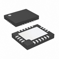
LT3751EUFD#PBF Linear Technology, LT3751EUFD#PBF Datasheet - Page 16

LT3751EUFD#PBF
Manufacturer Part Number
LT3751EUFD#PBF
Description
IC CAPACITOR CHRG 20-QFN
Manufacturer
Linear Technology
Datasheet
1.LT3751EUFDPBF.pdf
(34 pages)
Specifications of LT3751EUFD#PBF
Applications
Photoflash Capacitor Charger
Current - Supply
5.5mA
Voltage - Supply
4.75 V ~ 24 V
Operating Temperature
-40°C ~ 125°C
Mounting Type
Surface Mount
Package / Case
20-QFN
Primary Input Voltage
24V
No. Of Outputs
1
No. Of Pins
20
Operating Temperature Range
-40°C To +125°C
Msl
MSL 1 - Unlimited
Supply Voltage Range
4.75V To 24V
Termination Type
SMD
Rohs Compliant
Yes
Lead Free Status / RoHS Status
Lead free / RoHS Compliant
Available stocks
Company
Part Number
Manufacturer
Quantity
Price
APPLICATIONS INFORMATION
LT3751
The total propagation delay, t
factor that affects effi ciency and is the summation of gate
driver on-off propagation delays and the discharge time
associated with the secondary winding capacitance. There
are two effective methods to reduce the total propagation
delay. First, reduce the total capacitance on the secondary
winding, most notably the diode capacitance. Second,
reduce the total required NMOS gate charge. Figure 8
shows the effect of large secondary capacitance.
The energy stored in the secondary winding capacitance
is ½ • C
primary when the diode stops forward conduction. If the
refl ected capacitance is greater than the total NMOS drain
capacitance, the drain of the NMOS power switch goes
negative and its intrinsic body diode conducts. It takes
some time for this energy to be dissipated and thus adds
to the total propagation delay.
Choosing Regulator Maximum I
The I
on the desired maximum output power instead of charge
time like that in a capacitor charger application.
Note that the LT3751 regulation scheme varies the peak
current based on the output load current. The maximum
I
load conditions where output power is maximized.
16
PK
V
DRAIN
I
I
I
SEC
PK
PRI
is only reached during charge mode or during heavy
PK
Figure 8. Effect of Secondary Winding Capacitance
= 2 •
parameter in regulation mode is calculated based
NO SEC.
CAPACITANCE
SEC
P
Efficiency
OUT(AVG)
• V
OUT
2
. This energy is refl ected to the
SEC. DISCHARGE
•
⎛
⎝ ⎜
V
TRANS
d
, is the second most dominant
1
PK
+
V
OUT
N
⎞
⎠ ⎟
3751 F08
t
Transformer Design
The transformer’s primary inductance, L
by the desired V
parameters. Use the following equation to select L
The previous equation guarantees that the V
has enough time to sense the fl yback waveform and trip
the DONE pin latch. Operating V
than that used to calculate L
condition and overcharge the output capacitor.
The L
applications. Note that if both I
signifi cantly for a given V
I
will result in a lower than expected maximum output power.
To prevent this from occurring, maintain the condition in
the following equation.
The upper constraint on L
V
regulation occurs when operating the boundary-mode
frequency above 100kHz (refer to Operation section for
boundary-mode defi nition).
Figure 9 defi nes the maximum boundary-mode switching
frequency when operating at a desired output power level
and is normalized to L
of output power, boundary-mode frequency, I
primary inductance can be used as a guide throughout
the design process.
PK
TRANS
L
L
will not be reached within the refresh clock period. This
PRI
PRI
PRI
=
<
and starting the design process over. The best
I
3μs • V
PK
equation is adequate for most regulator
I
PK
•
⎡
⎢
⎣
•N
V
OUT
OUT
TRANS
38μs
1
and previously calculated N and I
PRI
/P
+
PRI
TRANS
OUT
V
OUT
PRI
N
can be reduced by increasing
(μH/Watt). The relationship
could result in a runaway
⎤
⎥
⎦
and V
PK
OUT
and N are increased
signifi cantly higher
OUT
PRI
, the maximum
OUT
, is determined
comparator
PK
PRI
, and
3751fb
:
PK


