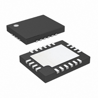
LT3751EUFD#PBF Linear Technology, LT3751EUFD#PBF Datasheet - Page 19

LT3751EUFD#PBF
Manufacturer Part Number
LT3751EUFD#PBF
Description
IC CAPACITOR CHRG 20-QFN
Manufacturer
Linear Technology
Datasheet
1.LT3751EUFDPBF.pdf
(34 pages)
Specifications of LT3751EUFD#PBF
Applications
Photoflash Capacitor Charger
Current - Supply
5.5mA
Voltage - Supply
4.75 V ~ 24 V
Operating Temperature
-40°C ~ 125°C
Mounting Type
Surface Mount
Package / Case
20-QFN
Primary Input Voltage
24V
No. Of Outputs
1
No. Of Pins
20
Operating Temperature Range
-40°C To +125°C
Msl
MSL 1 - Unlimited
Supply Voltage Range
4.75V To 24V
Termination Type
SMD
Rohs Compliant
Yes
Lead Free Status / RoHS Status
Lead free / RoHS Compliant
Available stocks
Company
Part Number
Manufacturer
Quantity
Price
APPLICATIONS INFORMATION
Gate Driver Operation
The LT3751 gate driver has an internal, selectable 10.5V
or 5.6V clamp with up to 2A current capability (using
LVGATE). For 10.5V operation, tie CLAMP pin to ground,
and for 5.6V operation, tie the CLAMP pin to the V
Choose a clamp voltage that does not exceed the NMOS
manufacturer’s maximum V
can also be used to reduce LT3751 power dissipation
and increase effi ciency when using logic-level FETs. The
typical gate driver overshoot voltage is 0.5V above the
clamp voltage.
The LT3751’s gate driver also incorporates a PMOS pull-up
device via the LVGATE pin. The PMOS pull-up driver should
only be used for V
LVGATE with V
to the part. LVGATE is active when tied to HVGATE and
allows rail-to-rail gate driver operation. This is especially
useful for low V
drive capability. It also provides the fastest rise times,
given the larger 2A current capability verses 1.5A when
using only HVGATE.
Output Diode Selection
The output diode(s) are selected based on the maximum
repetitive reverse voltage (V
current (I
V
I
current is also a function of the output voltage.
Table 4. Recommended Output Diodes
MANUFACTURER
Central Semiconductor
www.centralsemi.com
Fairchild Semiconductor
www.fairchildsemi.com
On Semiconductor
www.onsemi.com
Vishay
www.vishay.com
PK
OUT
/2N, the average short-circuit current. The average diode
+ N • V
F(AV)
TRANS
). The output diode’s V
CC
CC
CC
above 8V will cause permanent damage
. The output diode’s I
applications of 8V or below. Operating
applications, allowing better NMOS
RRM
GS
PART NUMBER
CMR1U-10M
CMSH2-60M
CMSH5-40
ES3J
ES1G
ES1J
MURS360
MURA260
MURA160
USB260
US1G
US1M
GURB5H60
) and the average forward
ratings. The 5.6V clamp
RRM
F(AV)
should exceed
should exceed
CC
pin.
I
F(AV)
1
2
5
3
1
1
3
2
1
2
1
1
5
The highest average diode current occurs at low output
voltages and decreases as the output voltage increases.
Reverse recovery time, reverse bias leakage and junction
capacitance should also be considered. All affect the overall
charging effi ciency. Excessive diode reverse recovery
times can cause appreciable discharging of the output
capacitor, thereby increasing charge time. Choose a diode
with a reverse recovery time of less than 100ns. Diode
leakage current under high reverse bias bleeds the output
capacitor of charge and increases charge time. Choose a
diode that has minimal reverse bias leakage current. Diode
junction capacitance is refl ected back to the primary, and
energy is lost during the NMOS intrinsic diode conduction.
Choose a diode with minimal junction capacitance. Table 4
recommends several output diodes for various output
voltages that have adequate reverse recovery times.
Setting Current Limit
Placing a sense resistor from the positive sense pin, CSP ,
to the negative sense pin, CSN, sets the maximum peak
switch current. The maximum current limit is nominally
106mV/R
resistor must exceed:
Additionally, there is approximately a 180ns propaga-
tion delay from the time that peak current limit is
(A)
I
P
AVG
RSENSE
=
SENSE
2 • (V
≥
V
I
RRM
2
1000
1000
I
. The power rating of the current sense
OUT
600
400
600
600
600
600
600
400
600
PK
60
40
PK
(V)
• R
• V
+ N • V
3
SENSE
TRANS
TRANS
⎛
⎜
⎝
V
T
OUT(PK)
RR
)
100
35
35
35
75
75
75
30
50
75
30
(ns)
V
OUT(PK)
+ N • V
LT3751
TRANS
PACKAGE
D
SMA
SMA
SMC
SMC
SMA
SMA
SMC
SMA
SMA
SMB
SMA
SMA
2
PAK
19
⎞
⎟
⎠
3751fb


