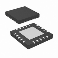
IR3088AMTRPBF International Rectifier, IR3088AMTRPBF Datasheet - Page 29

IR3088AMTRPBF
Manufacturer Part Number
IR3088AMTRPBF
Description
IC XPHASE W/FAULT DET 20L-MLPQ
Manufacturer
International Rectifier
Series
XPhase™r
Datasheet
1.IR3088AMTRPBF.pdf
(33 pages)
Specifications of IR3088AMTRPBF
Applications
Processor
Current - Supply
10mA
Voltage - Supply
8.4 V ~ 14 V
Operating Temperature
0°C ~ 125°C
Mounting Type
Surface Mount
Package / Case
20-MLPQ
Pin Count
20
Mounting
Surface Mount
Package Type
MLPQ
Case Length
4mm
Case Height
0.88mm
Lead Free Status / RoHS Status
Lead free / RoHS Compliant
Other names
IR3088AMTRPBF
IR3088AMTRPBFTR
IR3088AMTRPBFTR
Available stocks
Company
Part Number
Manufacturer
Quantity
Price
Part Number:
IR3088AMTRPBF
Manufacturer:
IR
Quantity:
20 000
LAYOUT GUIDELINES
The following layout guidelines are recommended to reduce the parasitic inductance and resistance of the PCB
layout, therefore minimizing the noise coupled to the IC.
• Dedicate at least one middle layer for a ground plane, which is then split into signal ground plane (LGND) and
• Connect PGND to LGND pins of each phase IC to the ground tab, which is tied to LGND and PGND planes
• In order to reduce the noise coupled to SCOMP pin of phase IC, use a dedicated wire to connect the capacitor
• Place current sense resistors and capacitors (R
• Place the decoupling capacitors C
• Place the phase IC as close as possible to the MOSFETs to reduce the parasitic resistance and inductance of
• Place the input ceramic capacitors close to the drain of top MOSFET and the source of bottom MOSFET. Use
• There are two switching power loops. One loop includes the input capacitors, top MOSFET, inductor, output
Page 29 of 33
power ground plane (PGND).
respectively through vias.
C
resistor R
connection for the inductor current sense wires, but separate the two wires by ground polygon. The wire from
the inductor terminal to RCS- should not cross over the fast transition nodes, i.e. switching nodes, gate drive
outputs and bootstrap nodes.
respectively.
the gate drive paths.
combination of different packages of ceramic capacitors.
capacitors and the load; another loop consists of bottom MOSFET, inductor, output capacitors and the load.
Route the switching power paths using wide and short traces or polygons; use multiple vias for connections
between layers.
SCOMP
directly to LGND pin. However, connect PWM ramp capacitor C
PHASE2
PLANE
PLANE
PLANE
PLANE
LGND
LGND
PGND
PGND
To PGND
To PGND
To LGND
To LGND
Plane
Plane
Plane
Plane
or R
PHASE3,
To VIN
To VIN
C
C
C
C
VCC
VCC
VCCL
VCCL
decoupling capacitor C
To LGND
To LGND
Plane
Plane
VCC
PWMRMP
PWMRMP
and C
SCOMP
SCOMP
LGND
LGND
EAIN
EAIN
VCC
VCC
VCCL
To Bottom
To Bottom
MOSFET
MOSFET
CS+
as close as possible to VCC and VCCL pins of the phase IC
To Signal Bus
To Signal Bus
VCC
, R
MOSFET
MOSFET
To Top
To Top
CS-
to LGND plane through vias.
, C
Switching
Switching
CS+
Node
Node
To
To
To LGND
To LGND
, and C
CSIN-
CSIN-
Plane
Plane
BIASIN
BIASIN
DACIN
DACIN
PHSFLT
PHSFLT
CSIN+
CSIN+
PWMRMP
CS-
) close to phase IC. Use Kelvin
To Inductor
To Inductor
Ground
Ground
Polygon
Polygon
, phase delay programming
IR3088APbF
To Gate
To Gate
Voltage
Voltage
Drive
Drive
May 18, 2009
Ground
Ground
Polygon
Polygon


