LM26480SQ-AA/NOPB National Semiconductor, LM26480SQ-AA/NOPB Datasheet - Page 4
LM26480SQ-AA/NOPB
Manufacturer Part Number
LM26480SQ-AA/NOPB
Description
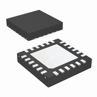
IC REG BUCK/LDO DUAL 1.5A 24LLP
Manufacturer
National Semiconductor
Specifications of LM26480SQ-AA/NOPB
Applications
Processor
Voltage - Supply
2.8 V ~ 5.5 V
Operating Temperature
-40°C ~ 85°C
Mounting Type
Surface Mount
Package / Case
24-LLP
Operating Temperature (max)
85C
Operating Temperature (min)
-40C
Pin Count
24
Mounting
Surface Mount
Package Type
LLP EP
Case Length
4mm
Screening Level
Industrial
For Use With
LM26480SQ-AAEV - BOARD EVALUATION LM26480SQ-AA
Lead Free Status / RoHS Status
Lead free / RoHS Compliant
Current - Supply
-
Lead Free Status / Rohs Status
Compliant
Other names
LM26480SQ-AATR
Available stocks
Company
Part Number
Manufacturer
Quantity
Price
Company:

Part Number:
LM26480SQ-AA/NOPB
Manufacturer:
TI
Quantity:
3 400
Part Number:
LM26480SQ-AA/NOPB
Manufacturer:
NS/国半
Quantity:
20 000


www.national.com
LLP Pin
Pin Descriptions
A: Analog Pin
VIN+ is the largest potential voltage on the device.
DAP
No.
10
11
12
13
14
15
16
17
18
19
20
21
22
23
24
1
2
3
4
5
6
7
8
9
Power Block Input
VINLDO12
AVDD
VIN1
VIN2
VINLDO1
VINLDO2
VINLDO12
GND_SW1
GND_SW2
VINLDO1
VINLDO2
ENLDO2
ENLDO1
ENSW1
GND_C
ENSW2
GND_L
NPOR
SYNC
AVDD
Name
LDO1
LDO2
FBL1
FBL2
VIN1
VIN2
SW1
SW2
DAP
FB1
FB2
D: Digital Pin
GND
I/O
G: Ground Pin
O
G
O
G
O
G
G
O
O
I
I
I
I
I
I
I
I
I
I
I
I
I
I
I
Enabled
VIN+
VIN+
VIN+
VIN+
≤
≤
VIN+
VIN+
Type
PWR
G/(D)
PWR
PWR
PWR
PWR
PWR
PWR
PWR
PWR
PWR
GND
D
G
D
G
D
G
D
D
G
A
A
A
A
PWR: Power Pin
Power Block Operation
Analog Power for Internal Functions (VREF, BIAS, I
Frequency Synchronization pin which allows the user to connect an external clock
signal to synchronize the PMIC internal oscillator. Default OFF and must be
grounded when not used. Part number LM26480SQ-BF has this feature enabled.
Please contact National Semiconductor Sales Office/Distributors for availability of
LM26480SQ-BF.
nPOR Power on reset pin for both Buck1 and Buck 2. Open drain logic output
100K pullup resistor. nPOR is pulled to ground when the voltages on these
supplies are not good. See nPOR section for more info.
Buck1 NMOS Power Ground
Buck1 switcher output pin
Power in from either DC source or Battery to Buck1
Enable Pin for Buck1 switcher, a logic HIGH enables Buck1. Pin cannot be left
floating.
Buck1 input feedback terminal
Non-switching core ground pin
Analog Power for Buck converters
Buck2 input feedback terminal
Enable Pin for Buck2 switcher, a logic HIGH enables Buck2. Pin cannot be left
floating.
Power in from either DC source or Battery to Buck2
Buck2 switcher output pin
Buck2 NMOS
LDO2 enable pin, a logic HIGH enables LDO2. Pin cannot be left floating.
LDO1 enable pin, a logic HIGH enables LDO1. Pin cannot be left floating.
LDO ground
Power in from either DC source or battery to LDO1
LDO1 Output
LDO1 Feedback Terminal
LDO2 Feedback Terminal
LDO Output
Power in from either DC source or battery to LDO2.
Connection isn't necessary for electrical performance, but it is recommended for
better thermal dissipation.
Disabled
VIN+
VIN+
VIN+ or 0V
VIN+ or 0V
≤
≤
VIN+
VIN+
I: Input Pin
4
I/O: Input/Output Pin
Description
Note
Always Powered
Always Powered
If Enabled, Min VIN is 1.74V
If Enabled, Min VIN is 1.74V
O: Output Pin
2
C, Logic)
Related parts for LM26480SQ-AA/NOPB
Image
Part Number
Description
Manufacturer
Datasheet
Request
R

Part Number:
Description:
BOARD EVALUATION LM26480SQ-AA
Manufacturer:
National Semiconductor
Datasheet:
Part Number:
Description:
EVAL BOARD FOR LM26LV
Manufacturer:
National Semiconductor
Datasheet:
Part Number:
Description:
LM26480 Q Automotive Version
Manufacturer:
National Semiconductor
Part Number:
Description:
LM26480 Q Automotive Version
Manufacturer:
National Semiconductor

Part Number:
Description:
Lm26480 Externally Programmable Dual High-current Step-down Dc/dc And Dual Linear Regulators
Manufacturer:
National Semiconductor Corporation
Datasheet:
Part Number:
Description:
National Semiconductor [8-Bit D/A Converter]
Manufacturer:
National Semiconductor
Datasheet:
Part Number:
Description:
National Semiconductor [Media Coprocessor]
Manufacturer:
National Semiconductor
Datasheet:
Part Number:
Description:
Digitally Controlled Tone and Volume Circuit with Stereo Audio Power Amplifier, Microphone Preamp Stage and National 3D Sound
Manufacturer:
National Semiconductor
Datasheet:
Part Number:
Description:
Digitally Controlled Tone and Volume Circuit with Stereo Audio Power Amplifier, Microphone Preamp Stage and National 3D Sound
Manufacturer:
National Semiconductor
Datasheet:
Part Number:
Description:
AC97 Rev 2 Codec with Sample Rate Conversion and National 3D Sound
Manufacturer:
National Semiconductor
Part Number:
Description:
Manufacturer:
National Semiconductor
Datasheet:
Part Number:
Description:
Manufacturer:
National Semiconductor
Datasheet:
Part Number:
Description:
General Purpose, Low Voltage, Low Power, Rail-to-Rail Output Operational Amplifiers
Manufacturer:
National Semiconductor
Datasheet:
Part Number:
Description:
8-bit 20 MSPS flash A/D converter.
Manufacturer:
National Semiconductor
Datasheet: