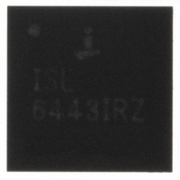
ISL6443IRZ Intersil, ISL6443IRZ Datasheet

ISL6443IRZ
Specifications of ISL6443IRZ
Available stocks
Related parts for ISL6443IRZ
ISL6443IRZ Summary of contents
Page 1
... MARKING RANGE (°C) ISL6443IR ISL6443IR - 5x5 QFN L28.5x5 ISL6443IRZ ISL6443IRZ - 5x5 QFN (See Note) (Pb-free) Add “-T” or “-TK” suffix for tape and reel. NOTE: Intersil Pb-free plus anneal products employ special Pb-free material sets; molding compounds/die attach materials and 100% matte tin plate termination finish, which are RoHS compliant and compatible with both SnPb and Pb-free soldering operations ...
Page 2
Pinouts ISL6443 (QFN) TOP VIEW PHASE2 1 ISEN2 2 PGOOD 3 VCC_5V 4 SD2 5 SS2 6 7 OCSET2 ISL6443 23 22 ISEN1 21 PGND 20 19 SD1 18 ...
Page 3
Block Diagram BOOT1 UGATE1 PHASE1 ADAPTIVE DEAD-TIME DIODE EMULATION VCC_5V V/I SAMPLE TIMING LGATE1 PGND 0.8V REFERENCE + GATE3 + FB3 18.5pF 1400kΩ 180kΩ FB1 - 16kΩ 0.8V ERROR AMP 1 ...
Page 4
Typical Application Schematic D1 BAT54HT1 C3 1µF C7 0.1µF L1 VOUT1 6.4µ +1.2V, 2A 330µ FDS6990S 4.99k R2 10K PGOOD 4 ISL6443 C2 4.7µF VIN VCC_5V SS1 SS2 0.1µF BOOT1 BOOT2 ...
Page 5
Absolute Maximum Ratings Supply Voltage (VCC_5V Pin -0.3V to +7V Input Voltage (V Pin ...
Page 6
Electrical Specifications Recommended operating conditions unless otherwise noted. Refer to Block Diagram and Typical Application Schematic. V Typical values are at T PARAMETER PWM CONVERTERS Output Voltage FB Pin Bias Current Maximum Duty Cycle Minimum Duty Cycle PWM CONTROLLER ERROR ...
Page 7
Electrical Specifications Recommended operating conditions unless otherwise noted. Refer to Block Diagram and Typical Application Schematic. V Typical values are at T PARAMETER PROTECTION Thermal Shutdown NOTES: 2. Specifications at -40°C and 85°C are guaranteed by design, not production tested. ...
Page 8
Typical Performance Curves (Oscilloscope Plots are Taken Using the ISL6443EVAL Evaluation Board, VIN = 12V Unless Otherwise Noted.) 3.4 3.39 3.38 3.37 3.36 3.35 3.34 3.33 3.32 3.31 3.3 0 0.5 1 1.5 2 2.5 LOAD CURRENT (A) FIGURE 1. ...
Page 9
Typical Performance Curves (Oscilloscope Plots are Taken Using the ISL6443EVAL Evaluation Board, VIN = 12V Unless Otherwise Noted.) V 200mV/DIV OUT1 AC COUPLED I 1A/DIV OUT1 FIGURE 7. LOAD TRANSIENT RESPONSE VOUT1 (3.3V) VCC_5V 1V/DIV V 1V/DIV OUT1 FIGURE 9. ...
Page 10
Pin Descriptions BOOT2, BOOT1 - These pins power the upper MOSFET drivers of each PWM converter. Connect this pin to the junction of the bootstrap capacitor and the cathode of the bootstrap diode. The anode of the bootstrap diode is ...
Page 11
Functional Description General Description The ISL6443 integrates control circuits for two synchronous buck converters and one linear controller. The two synchronous bucks operate out of phase to substantially reduce the input ripple and thus reduce the input filter requirements. The ...
Page 12
Out-of-Phase Operation The two PWM controllers in the ISL6443 operate 180 phase to reduce input ripple current. This reduces the input capacitor ripple current requirements, reduces power supply- induced noise, and improves EMI. This effectively helps to lower component cost, ...
Page 13
I is the desired overcurrent protection threshold, OC and value of the current sense resistor connected CS to the ISENx pin overcurrent is detected for 2 consecutive clock cycles then the IC enters a ...
Page 14
CONVERTER 17.5dB M G MODULATOR FIGURE 17. FEEDBACK LOOP COMPENSATION The zero frequency, the amplifier high-frequency gain, and the modulator gain are chosen to satisfy most typical applications. The crossover ...
Page 15
EMI onto the base drive causes fluctuations in the base current, which appear as noise on the linear regulator’s output. Keep the base drive traces away from the step-down converter, and as short as possible, to minimize noise coupling. A ...
Page 16
– OUT P ------------------------------------------------------------------------------ - = LOWER large gate-charge increases the switching time, t which increases the upper MOSFET switching losses. ...
Page 17
... Accordingly, the reader is cautioned to verify that data sheets are current before placing orders. Information furnished by Intersil is believed to be accurate and reliable. However, no responsibility is assumed by Intersil or its subsidiaries for its use; nor for any infringements of patents or other rights of third parties which may result from its use ...
Page 18
... Dimensions D2 and E2 are for the exposed pads which provide improved electrical and thermal performance. 8. Nominal dimensions are provided to assist with PCB Land Pattern Design efforts, see Intersil Technical Brief TB389. 9. Features and dimensions A2, A3, D1, E1, P & θ are present when C L Anvil singulation method is used and not present for saw singulation ...


