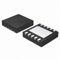
LT3585EDDB-2#TRPBF Linear Technology, LT3585EDDB-2#TRPBF Datasheet - Page 13

LT3585EDDB-2#TRPBF
Manufacturer Part Number
LT3585EDDB-2#TRPBF
Description
IC CHARGER PHOTOFLASH 10-DFN
Manufacturer
Linear Technology
Datasheet
1.LT3585EDDB-2TRPBF.pdf
(20 pages)
Specifications of LT3585EDDB-2#TRPBF
Applications
Photoflash Capacitor Charger, Xenon
Current - Supply
5mA
Voltage - Supply
1.5 V ~ 16 V
Operating Temperature
-40°C ~ 85°C
Mounting Type
Surface Mount
Package / Case
10-DFN
Lead Free Status / RoHS Status
Lead free / RoHS Compliant
Available stocks
Company
Part Number
Manufacturer
Quantity
Price
IGBT Drive
The IGBT is a high current switch for the 100A+ current
through the photofl ash lamp. To create a redeye effect or
to adjust the light output, the lamp current needs to be
stopped or quenched with an IGBT before discharging
the photofl ash capacitor fully. The IGBT device also con-
trols the 4kV trigger pulse required to ionize the Xenon
gas in the photofl ash lamp. Figure 8 is a schematic of a
fully functional photofl ash application with the LT3585-0
serving as the IGBT driver. An IGBT driver charges the
gate capacitance to start the fl ash. The IGBT driver does
not need to pull up the gate signifi cantly fast because of
the inherently slow nature of the IGBT. A rise time of 2µs
is suffi cient to charge the gate of the IGBT and create a
trigger pulse. With slower rise times, the trigger circuitry
will not have a fast enough edge to create the required
4kV pulse. The fall time of the IGBT driver is critical to the
APPLICATIO S I FOR ATIO
Table 3. Recommended Output Diodes
PART
GSD2004S
(DUAL DIODE)
CMSD2004S
(DUAL DIODE)
MMBD3004S
(DUAL DIODE)
IGBTOUT
IGBTIN
1V/DIV
2V/DIV
Figure 6. IGBT Driver Output with 4000pF Load
I
C
R
GBTPWR
OUT
PD
= 50Ω
= 4000pF
= 5V
U
500ns/DIV
U
MAX REVERSE
VOLTAGE (V)
2 × 300
2 × 300
2 × 350
W
3585 F06
U
FORWARD CURRENT (mA)
MAX CONTINUOUS
225
225
225
safe operation of the IGBT. The IGBT gate is a network of
resistors and capacitors, as shown in Figure 9. When the
gate terminal is pulled low, the capacitance closest to the
terminal goes low but the capacitance further from the
terminal remains high. This causes a smaller portion of
the device to handle a larger portion of the current, which
can damage the device. The pull-down circuitry needs to
pull down slower than the internal RC time constant in
the gate of the IGBT. This is easily accomplished with a
resistor placed in series with the IGBTPD pin.
The LT3585 series integrated IGBT drive circuit is indepen-
dent of the charging function and draws its power from
the IGBTPWR pin. The drive pulls high to within 200mV
of IGBTPWR and pulls down to 100mV. The circuit’s
switching waveform is shown in Figure 6. The rise and fall
times are measured using a 4000pF output capacitor. The
typical 10% to 90% rise time is 320ns when IGBTPWR
1.2
2.0
1.8
1.6
1.4
1.0
0.8
0.6
0.4
0.2
0
Figure 7. IGBT Turn-Off Delay vs R
0
CAPACITANCE (pF)
LT3585-0/LT3585-1
LT3585-2/LT3585-3
50
5
5
5
R
PD
100
(Ω)
VENDOR
Vishay
(402) 563-6866
www.vishay.com
Central Semiconductor
(631) 435-1110
www.centralsemi.con
Diodes, Inc
(816) 251-8800
www.diodes.com
150
3585 F07
200
PD
13
3585f


