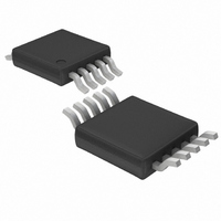
LT3420EMS-1#TRPBF Linear Technology, LT3420EMS-1#TRPBF Datasheet - Page 6

LT3420EMS-1#TRPBF
Manufacturer Part Number
LT3420EMS-1#TRPBF
Description
IC PHOTOFLASH CAP CHARGER 10MSOP
Manufacturer
Linear Technology
Datasheet
1.LT3420EMS.pdf
(20 pages)
Specifications of LT3420EMS-1#TRPBF
Applications
Photoflash Capacitor Charger
Current - Supply
90µA
Voltage - Supply
2.2 V ~ 16 V
Operating Temperature
-40°C ~ 85°C
Mounting Type
Surface Mount
Package / Case
10-MSOP, Micro10™, 10-uMAX, 10-uSOP
Lead Free Status / RoHS Status
Lead free / RoHS Compliant
Available stocks
Company
Part Number
Manufacturer
Quantity
Price
PI FU CTIO S
LT3420/LT3420-1
R
from the R
V
connected to the power supply or battery, which supplies
power to transformer T1. Must be locally bypassed.
R
from the SW pin to the R
following formula:
V
with a 4.7µF or larger ceramic capacitor.
6
BAT
CC
REF
FB
V
N: Transformer Turns Ratio
R
V
R2: Resistor from the R
Choice
R
R
U
OUT
D
(Pin 3): Feedback Resistor Pin. Place a resistor (R1)
SEC
1
(Pin 4): Input Supply Pin. Must be locally bypassed
1
(Pin 1): Reference Resistor Pin. Place a resistor (R2)
: Diode Forward Voltage Drop
(Pin 2): Battery Voltage Input. This pin should be
=
=
: Transformer Secondary Resistance
R
R
N
N
: Desired Output Voltage
2
2
2
2
U
REF
[
[
(
( . •
1 4
R
pin to GND. 2k is recommended.
SEC
R
)
SEC
+
U
N V
(
)
+
OUT
FB
N V
REF
(
pin. Set R1 according to the
+
OUT
Pin to GND. 2k is a Typical
2
V
D
+
) (LT3420-1)
]
2
V
D
) (LT3420)
]
GND (Pin 5): Ground. Tie directly to local ground plane.
SW (Pin 6): Switch Pin. This is the collector of the internal
NPN power switch. Minimize the metal trace area con-
nected to this pin to minimize EMI.
SEC (Pin 7): Transformer Secondary Pin. Tie one end of
the transformer secondary to this pin. Take care to use the
correct phasing of the transformer (Refer to Figures 1
and 2).
DONE (Pin 8): Done Output Pin. Open collector NPN
output. DONE is pulled low whenever the chip is delivering
power to the output and goes high when power delivery
stops.
CHARGE (Pin 9): Charge Pin. Drive CHARGE high (1.5V or
more) to commence charging of the output capacitor.
Drive to 0.2V or less to put the part in shutdown mode.
C
from the C
according to the following formula:
EXPOSED PAD (Pin 11) (DD Package only): GND. Must be
soldered to local ground plane on PCB.
T
C
t
(Pin 10): Refresh Timer Capacitor Pin. Place a capacitor
REFRESH
T
= 2.5 • 10
T
: Desired Refresh Period in Seconds.
pin to GND to set the refresh timer sample rate
–6
• t
REFRESH
3420fb


