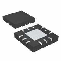
MAX8890ETCDDD+ Maxim Integrated Products, MAX8890ETCDDD+ Datasheet - Page 7

MAX8890ETCDDD+
Manufacturer Part Number
MAX8890ETCDDD+
Description
IC POWER MANAGE CELL 12-TQFN
Manufacturer
Maxim Integrated Products
Datasheet
1.MAX8890ETCAAAT.pdf
(12 pages)
Specifications of MAX8890ETCDDD+
Applications
Handheld/Mobile Devices
Current - Supply
180µA
Voltage - Supply
2.5 V ~ 5.5 V
Operating Temperature
-40°C ~ 85°C
Mounting Type
Surface Mount
Package / Case
12-TQFN Exposed Pad
Product
Charge Management
Battery Type
Li-Ion, Li-Polymer
Operating Supply Voltage
2.5 V to 5.5 V
Supply Current
180 uA
Maximum Operating Temperature
+ 85 C
Minimum Operating Temperature
- 40 C
Charge Safety Timers
No
Mounting Style
SMD/SMT
Temperature Monitoring
No
Uvlo Start Threshold
2.25 V
Uvlo Stop Threshold
2.25 V
Lead Free Status / RoHS Status
Lead free / RoHS Compliant
The MAX8890 is an RF power-management IC for a
cellular phone. The MAX8890 contains three low-noise,
low quiescent current, low-dropout, linear regulators for
powering the transmitter, receiver, synthesizer, TCXO,
and voltage controlled oscillators (VCOs). Each low-
dropout linear regulator (LDO) supplies loads up to
100mA and is available with preset output voltages
from 1.8V to 3.3V in 50mV increments. Furthermore, the
MAX8890’s input voltage range of 2.5V to 5.5V is per-
fect for single-cell Li+ battery or 3-cell NiMH battery
applications.
As illustrated in Figure 2, each regulator consists of an
error amplifier, internal feedback resistive-divider, and
P-channel MOSFET pass transistor. The output voltage
feeds back through the internal resistive-divider con-
nected to OUT_. This feedback voltage connects to the
error amplifier, which compares the feedback voltage
with the internal 1.25V reference voltage and amplifies
the difference. If the feedback voltage is lower than the
reference voltage, the pass-transistor gate is pulled
lower, which allows more current to flow to the output
and increases the output voltage. If the feedback volt-
age is too high, the pass-transistor gate is pulled up,
allowing less current to flow to the output.
Clear transmission and reception in a cellular phone
can only be achieved with a low-noise power supply.
Therefore, all three LDOs on the MAX8890 feature low
output voltage noise, high power-supply rejection
ratios, and excellent load and line regulation character-
istics. Designed for single-cell Li+ battery applications
where a pulsed current demand is required from the
Figure 1. Typical Application Circuit
_______________________________________________________________________________________
Detailed Description
2.5V TO 5.5V
INPUT
4.7 F
ON
C
OFF
IN
Integrated Cellular RF-Section
IN1
IN2
IN3
EN1
EN2
EN3
MAX8890
OUT1
OUT2
OUT3
GND
BP
battery, each LDO is designed with 45µV
from 10Hz to 100kHz and PSRR of 67dB.
The MAX8890 also features output current limiting
(short-circuit protection), a low-power shutdown mode,
and thermal overload protection.
Each linear regulator features a 0.5 P-channel MOSFET
pass transistor. Unlike similar designs using PNP pass
transistors, P-channel MOSFETs require no base drive,
which reduces the quiescent current. PNP based regula-
tors also waste considerable current in dropout when the
pass transistor saturates and use high base-drive cur-
rents under large loads. The MAX8890 does not suffer
from these problems and consumes only 180µA of quies-
cent current (all three regulators enabled).
The MAX8890 contains separate current-limit circuitry
for each linear regulator. The device monitors and con-
trols the gate voltage of each pass transistor, limiting
the regulator’s output current to 250mA (typ). The out-
put can be shorted to ground for an indefinite period of
time without damage to the part as long as the maxi-
mum continuous power dissipation rating is not
exceeded.
The MAX8890 is supplied with factory-set output volt-
ages from 1.8V to 3.3V in 50mV increments. The three-
letter part number suffix identifies the output voltage for
each regulator. For example, the MAX8890ETCAKM’s
output voltages are preset to 3.3V (V
(V
Power-Management IC
OUT2
C
2.2 F
C
0.01 F
OUT1
BP
Current Limit (Short-Circuit Protection)
C
2.2 F
), and 1.8V (V
OUT2
C
2.2 F
OUT3
Internal P-Channel Pass MOSFET
OUTPUT #1
(1.8V TO 3.3V)*
OUTPUT #2
(1.8V TO 3.3V)*
OUTPUT #3
(1.8V TO 3.3V)*
*See the Ordering Information and
Standard Preset Output Voltage Suffixes sections
OUT3
Output Voltage Selection
).
OUT1
RMS
), 2.5V
noise
7


