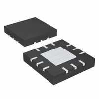
MAX8890ETCDDD+ Maxim Integrated Products, MAX8890ETCDDD+ Datasheet - Page 9

MAX8890ETCDDD+
Manufacturer Part Number
MAX8890ETCDDD+
Description
IC POWER MANAGE CELL 12-TQFN
Manufacturer
Maxim Integrated Products
Datasheet
1.MAX8890ETCAAAT.pdf
(12 pages)
Specifications of MAX8890ETCDDD+
Applications
Handheld/Mobile Devices
Current - Supply
180µA
Voltage - Supply
2.5 V ~ 5.5 V
Operating Temperature
-40°C ~ 85°C
Mounting Type
Surface Mount
Package / Case
12-TQFN Exposed Pad
Product
Charge Management
Battery Type
Li-Ion, Li-Polymer
Operating Supply Voltage
2.5 V to 5.5 V
Supply Current
180 uA
Maximum Operating Temperature
+ 85 C
Minimum Operating Temperature
- 40 C
Charge Safety Timers
No
Mounting Style
SMD/SMT
Temperature Monitoring
No
Uvlo Start Threshold
2.25 V
Uvlo Stop Threshold
2.25 V
Lead Free Status / RoHS Status
Lead free / RoHS Compliant
When the junction temperature exceeds T
thermal sensor activates the shutdown logic, disabling
the overheated regulator. The thermal sensor turns the
linear regulator on again after the regulator’s junction
temperature cools by 15°C, resulting in a pulsed output
during continuous thermal-overload conditions. For
continuous operation, do not exceed the absolute maxi-
mum junction-temperature rating of T
Capacitors are required at each input and each output
of the MAX8890 for stable operation over the full load
range and full temperature range. Connect a minimum
2.2µF ceramic capacitor between OUT_ and ground to
ensure stability and optimum transient response. Use
larger 10µF ceramic output capacitors for lower noise
requirements.
The input capacitor (C
ance of the input supply, thereby reducing the input
noise and improving transient response. Connect a
minimum 1µF ceramic capacitance between each IN_
and ground. Place all input and output capacitors as
close to the MAX8890 as possible to minimize the
impact of PC board trace impedance. Because IN1
and IN2 are next to each other, they may easily share a
single 2.2µF or larger ceramic capacitor.
Surface-mount ceramic capacitors have very low ESR
and are commonly available in values up to 10µF.
However, note that some ceramic dielectrics exhibit
large capacitance and ESR variation with temperature.
Z5U and Y5V dielectrics may require a minimum 3.3µF
nominal output capacitance, especially with low tem-
perature operation.
An external bypass capacitor is connected to BP to
reduce the inherent reference noise. The capacitor
forms a lowpass filter in conjunction with an internal
network. Use a 0.01µF or greater ceramic capacitor
connected as close to BP as possible. Capacitance
values greater than 0.01µF will increase the startup
time. (See Typical Operating Characteristics for startup
waveforms.) For the lowest noise, increase the bypass
capacitor to 0.1µF. Values above 0.1µF provide no per-
formance improvement and are therefore not recom-
mended. Do not place any additional loading on this
reference bypass pin.
Capacitor Selection and Regulator
Applications Information
_______________________________________________________________________________________
Reference Bypass Capacitor
IN
_) lowers the source imped-
J
= 150°C.
Integrated Cellular RF-Section
J
= 160°C, a
Stability
The MAX8890 is designed to operate with low dropout
voltages and low quiescent currents in battery-powered
systems while providing low noise, fast transient
response, and high AC rejection. See the Typical
Operating Characteristics for a plot of Power-Supply
Rejection Ratio (PSRR) vs. Frequency. When operating
from noisy sources, improved supply-noise rejection
and transient response can be achieved by increasing
the values of the input and output bypass capacitors
and through passive filtering techniques.
The MAX8890 load-transient response graphs (see
Typical Operating Characteristics) show two compo-
nents of the output response: a DC shift from the output
impedance due to the load current change and the
transient response. Increasing the output capacitor’s
value and decreasing the ESR reduces the transient
under/overshoot.
A regulator’s minimum input-to-output voltage differen-
tial (dropout voltage) determines the lowest useable
input supply voltage. Once the linear regulator reaches
dropout, the series pass transistor is fully on and regu-
lation ceases. The output voltage tracks the input volt-
age as the input voltage drops lower. Because the
MAX8890 uses P-channel MOSFET pass transistors, its
dropout voltage is a function of the MOSFET’s drain-to-
source on-resistance (R
current (see Typical Operating Characteristics):
Power-Management IC
V
DROPOUT
Noise, PSRR, and Transient Response
Input-Output (Dropout) Voltage
= V
IN
_ - V
DS(ON)
OUT
_ = R
) multiplied by the load
DS(ON)
I
OUT
_
9


