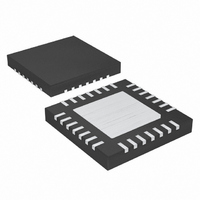
MAX8819AETI+T Maxim Integrated Products, MAX8819AETI+T Datasheet - Page 2

MAX8819AETI+T
Manufacturer Part Number
MAX8819AETI+T
Description
IC PMIC W/INT CHARGER 28TQFN-EP
Manufacturer
Maxim Integrated Products
Datasheet
1.MAX8819CETIT.pdf
(29 pages)
Specifications of MAX8819AETI+T
Applications
Handheld/Mobile Devices
Voltage - Supply
4.1 V ~ 5.5 V
Operating Temperature
-40°C ~ 85°C
Mounting Type
Surface Mount
Package / Case
28-TQFN Exposed Pad
Lead Free Status / RoHS Status
Lead free / RoHS Compliant
Current - Supply
-
Lead Free Status / Rohs Status
Lead free / RoHS Compliant
PMIC with Integrated Chargers and Smart
Power Selector in a 4mm x 4mm TQFN
ABSOLUTE MAXIMUM RATINGS
DC, SYS, BAT, CISET, DLIM1, DLIM2, EN123
PV2 to GND ...............................................-0.3V to (V
PV13 to SYS...........................................................-0.3V to +0.3V
PG1, PG2, PG3, PG4 to GND................................-0.3V to +0.3V
COMP4, FB4 to GND ................................-0.3V to (V
LX4 to PG4 .............................................................-0.3V to +33V
OVP4 to GND .........................................................-0.3V to +33V
LX1, LX2, LX3 Continuous Current (Note 1) .........................1.5A
LX4 Current ................................................................750mA
Output Short-Circuit Duration.....................................Continuous
ELECTRICAL CHARACTERISTICS
(DC, LX_ unconnected; V
PV13 = PV2 = SYS, T
Note 1: LX1, LX2, LX3 have clamp diodes to their respective PG_ and PV_. Applications that forward bias these diodes must take
Note 2: Package thermal resistances were obtained using the method described in JEDEC specification JESD51-7, using a four-layer
Stresses beyond those listed under “Absolute Maximum Ratings” may cause permanent damage to the device. These are stress ratings only, and functional
operation of the device at these or any other conditions beyond those indicated in the operational sections of the specifications is not implied. Exposure to
absolute maximum rating conditions for extended periods may affect device reliability.
2
DC POWER INPUT
DC Voltage Range
SYS Regulation Voltage
DC Undervoltage Threshold
DC Overvoltage Threshold
DC Current Limit
(Note 4)
DC Quiescent Current
DC-to-SYS Dropout Resistance
DC-to-SYS Soft-Start Time
DC Thermal-Limit Temperature
DC Thermal-Limit Gain
SYSTEM
System Operating Voltage Range
CEN, EN4, CHG, RST1, FB1, FB2, FB3 to GND....-0.3V to +6V
_______________________________________________________________________________________
care not to exceed the package power dissipation limits.
board. For detailed information on package thermal considerations, refer to http://www.maxim-ic.com/thermal-tutorial.
PARAMETER
A
= -40°C to +85°C, capacitors as shown in Figure 1, R
EP
= V
GND
= 0V, V
V
V
V
SYMBOL
UVLO_DC
OVLO_DC
SYS_REG
I
t
DCLIM
I
SS-D-S
V
V
DCIQ
R
SYS
DC
DS
BAT
= 4V, DLIM[1:2] = 00, EN123 = EN4 = low, V
V
V
V
V
for MAX8819B or V
4V for MAX8819A/
MAX8819C
DLIM[1:2] = 11 (suspend)
DLIM[1:2] ≠ 11, I
EN123 = low, EN4 = low, CEN = high,
V
DLIM[1:2] ≠ 11, I
EN4 = low, CEN = low, V
V
Die temperature where current limit is
reduced
Amount of input current reduction above
thermal-limit temperature
DC
DC
DC
DC
DC
DC
SYS
SYS
= 5.75V
rising, 500mV typical hysteresis
rising, 300mV typical hysteresis
= 5.75V, V
= 5.5V
= 4V, I
+ 0.3V)
+ 0.3V)
RMS
SYS
CONDITIONS
SYS
= 400mA, DLIM[1:2] = 01
SYS
SYS
SYS
= 5V
Continuous Power Dissipation (T
Junction-to-Case Thermal Resistance (θ
Operating Temperature Range ...........................-40°C to +85°C
Junction Temperature........................................-40°C to +125°C
Storage Temperature.........................................-65°C to +150°C
Lead Temperature (soldering, 10s) .................................+300°C
MAX8819A/MAX8819C
MAX8819B
= 0mA, I
= 0mA, EN123 = low,
28-Pin Thin QFN Single-Layer Board (derate 20.8mW/°C
above +70°C)...........................................................1666.7mW
28-Pin Thin QFN Multilayer Board (derate 28.6mW/°C
above +70°C)...........................................................2285.7mW
28-Lead Thin QFN...........................................................3°C/W
=
DC
CISET
= 5.5V
DLIM[1:2] = 10
DLIM[1:2] = 01
DLIM[1:2] = 00
BAT
= 3kΩ, unless otherwise noted.) (Note 3)
= 0mA,
FB1
5.811
= V
MIN
3.95
450
900
4.1
4.3
5.1
2.6
90
FB2
A
= +70°C)
= V
0.330
1000
TYP
4.35
4.00
0.02
1.33
0.95
475
100
5.3
5.9
1.5
95
FB3
5
JC
) (Note 2)
= 1.1V, V
6.000
0.035
0.700
MAX
1100
4.05
100
500
5.5
4.4
5.5
5.5
FB4
UNITS
%/°C
= 0.6V,
mA
mA
ms
°C
Ω
V
V
V
V
V


