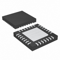
MAX8819AETI+T Maxim Integrated Products, MAX8819AETI+T Datasheet - Page 27

MAX8819AETI+T
Manufacturer Part Number
MAX8819AETI+T
Description
IC PMIC W/INT CHARGER 28TQFN-EP
Manufacturer
Maxim Integrated Products
Datasheet
1.MAX8819CETIT.pdf
(29 pages)
Specifications of MAX8819AETI+T
Applications
Handheld/Mobile Devices
Voltage - Supply
4.1 V ~ 5.5 V
Operating Temperature
-40°C ~ 85°C
Mounting Type
Surface Mount
Package / Case
28-TQFN Exposed Pad
Lead Free Status / RoHS Status
Lead free / RoHS Compliant
Current - Supply
-
Lead Free Status / Rohs Status
Lead free / RoHS Compliant
EN4 enables REG4, disables REG4, and adjusts the volt-
age on FB4 in 32 linear steps. If current adjustment is not
required, EN4 acts as a simple enable/disable controller.
Driving EN4 high for at least 100μs powers up REG4 and
sets V
ables REG4. To adjust V
Figure 8. Dim the WLEDs by pulsing EN4 low (500ns to
500μs pulse width). Each pulse reduces the LED current
by 1/32. Note: When REG4 is disabled, OUT4 is equal to
V
In the event that the load (typically WLEDs) opens,
V
tection threshold (typically 25V). When this occurs,
REG4 stops switching and latches off until EN4 is reset
low for at least 2ms.
The WLED boost converter switches at 1MHz, allowing
the use of a small inductor. A 10μH inductance value is
recommended for most applications. Smaller induc-
tances require less PCB space.
Use inductors with a ferrite core or equivalent.
Powdered iron cores are not recommended for use at
high-switching frequencies. The inductor’s saturation
current rating should preferably exceed the REG4
n-channel current limit of 700mA. Choose an inductor
with a DC resistance less than 300mΩ to maintain high
efficiency. Table 4 lists recommended inductors.
The REG4 diode must be fast enough to support the
switching frequency (1MHz). Schottky diodes, such as
Central Semiconductor’s CMHSH5-4 or ON Semicon-
ductor’s MBR0530L, are recommended. Make sure that
the diode’s peak-current rating matches or exceeds the
700mA REG4 n-channel current limit. The diode’s aver-
age current rating should match or exceed the output
current. The diode’s reverse breakdown voltage must
exceed the voltage from the converter’s output to
ground. Schottky diodes are preferred due to their low
forward voltage, however, ultra high-speed silicon recti-
fiers are also acceptable.
For most applications, a 0.1μF ceramic output filter
capacitor is suitable. Choose a voltage rating double
the maximum output voltage to minimize the effect of
the voltage coefficient on decreasing the effective
capacitance. To ensure stability over a wide tempera-
ture range, ceramic capacitors with an X5R or X7R
dielectric are recommended. Place these capacitors as
close as possible to the IC.
SYS
OUT4
minus the drop from the catch diode.
FB4
Step-Up Converter Output Capacitor Selection
rises quickly until it reaches the overvoltage pro-
to 0.5V. Pulling EN4 low for at least 2ms dis-
PMIC with Integrated Chargers and Smart
Step-Up Converter Inductor Selection
______________________________________________________________________________________
Step-Up Converter Diode Selection
Power Selector in a 4mm x 4mm TQFN
FB4
, apply pulses as shown in
The MAX8819_ implements soft-start on many levels to
control inrush current to avoid collapsing supply volt-
ages, and to fully comply with the USB 2.0 specifica-
tions. All DC and charging functions implement soft-start.
The DC node only requires 4.7μF of input capacitance.
Furthermore, all regulators implement soft-start to avoid
transient overload of power inputs.
DC undervoltage lockout (UVLO) prevents an input sup-
ply from being used when its voltage is below the oper-
ating range. When the voltage from DC to GND (V
less than the DC UVLO threshold (4.0V, typ), the DC
input is disconnected from SYS, the battery charger is
disabled and CHG is high impedance. BAT is connected
to SYS through the internal system load switch in DC
UVLO mode, allowing the battery to power the SYS
node. REG1–REG4 and the LED current sinks are
allowed to operate from the battery in DC UVLO mode.
DC overvoltage lockout (OVLO) is a fail-safe mecha-
nism and prevents an input supply from being used
when its voltage exceeds the operating range. The
absolute maximum ratings state that DC withstands
voltages up to 6V. Systems must be designed so that
DC never exceeds 6V (transient and steady-state). If
the voltage from DC to GND (V
DC OVLO threshold (5.9V typ) during a fault, the DC
input is disconnected from SYS, the battery charger is
disabled, and CHG is high impedance. BAT is connect-
ed to SYS through the internal system load switch in DC
OVLO mode, allowing the battery to power SYS through
the internal system load switch in DC OVLO mode.
REG1–REG4 are allowed to operate from the battery in
DC OVLO mode. Normal operation resumes when V
falls within its normal operating range.
SYS undervoltage lockout (UVLO) prevents the regula-
tors from being used when the input voltage is below
the operating range. When the voltage from SYS to
GND (V
typ), REG1–REG4, the LED current sinks, and the bat-
tery charger are disabled. Additionally, CHG, is high
impedance and RST1 is asserted.
The IC reduces the DC current limit by 5%/°C when the
die temperature exceeds +100°C. The system load
(I
Smart Power Selector Thermal-Overload Protection
Thermal Limiting and Overload Protection
SYS
Undervoltage and Overvoltage Conditions
) has priority over the charger current, so input
SYS
) is less than the SYS UVLO threshold (2.5V,
Soft-Start/Inrush Current
DC
) should exceed the
SYS UVLO
DC OVLO
DC UVLO
DC
) is
DC
27


