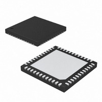
MAX8588ETM+T Maxim Integrated Products, MAX8588ETM+T Datasheet - Page 24

MAX8588ETM+T
Manufacturer Part Number
MAX8588ETM+T
Description
IC PMIC HI EFF LOW IQ 48-TQFN
Manufacturer
Maxim Integrated Products
Datasheet
1.MAX8588ETMT.pdf
(31 pages)
Specifications of MAX8588ETM+T
Applications
Processor
Voltage - Supply
2.6 V ~ 5.5 V
Operating Temperature
-40°C ~ 85°C
Mounting Type
Surface Mount
Package / Case
48-TQFN Exposed Pad
Lead Free Status / RoHS Status
Lead free / RoHS Compliant
Current - Supply
-
Lead Free Status / Rohs Status
Lead free / RoHS Compliant
A useful approximation is that it takes approximately 2.2
RC time constants for V3 to move from 10% to 90% of
the voltage difference. For C
is 330µs. For a 1V to 1.3V change, this equates to
1mV/µs. See the Typical Operating Characteristics for
examples of different ramp-rate settings.
The maximum capacitor value that can be used at
RAMP is 2200pF. If larger values are used, the V3 ramp
rate is still controlled according to the above equation,
but when V3 is first activated, POK indicates an “in reg-
ulation” condition before V3 reaches its final voltage.
The RAMP pin is effectively the reference for REG3.
FB3 regulates to 1.28 times the voltage on RAMP.
The outputs V1 and V2 have preset output voltages, but
can also be adjusted using a resistor voltage-divider. To
set V1 to 3.3V, connect FB1 to GND. V2 can be preset to
3.3V or 2.5V. To set V2 to 3.3V, connect FB2 to IN. To set
to 2.5V, connect FB2 to GND.
To set V1 or V2 to other than the preset output voltages,
connect a resistor voltage-divider from the output volt-
age to the corresponding FB input. The FB_ input bias
current is less than 100nA, so choose the low-side (FB_-
to-GND) resistor (R
late the high-side (output-to-FB_) resistor (R
The V3 (VCC_CORE) output voltage is set from 0.7V to
1.475V in 25mV steps by the I
the Serial Interface section for details.
Linear regulator V4 provides a fixed 1.3V output volt-
age. Linear regulator V5 provides a fixed 1.1V output
voltage. V4 and V5 voltages are not adjustable.
The output voltage of linear regulator V6 (VCC_USIM) is
set to 0V, 1.8V, 2.5V, or 3.0V by the I
See the Serial Interface section for details.
Linear regulator V7 (VCC_BATT) tracks the voltage at
V1 as long as ON1 is high and V1 is in regulation. When
ON1 is low or V1 is not in regulation, V7 switches to the
backup battery (V
The external components required for the step-down
are an inductor, input-and-output filter capacitors, and
a compensation RC network.
High-Efficiency, Low-I
Dynamic Core for PDAs and Smartphones
24
______________________________________________________________________________________
R
H
= R
BKBT
L
Setting the Output Voltages
) to be 100kΩ or less. Then calcu-
L
).
[(V
OUT
Design Procedure
RAMP
/ 1.25) – 1]
2
Inductor Selection
C serial interface. See
= 1500pF, this time
2
C serial interface.
H
) using:
Q
PMIC with
The MAX8588 step-down converter provides its best
efficiency with continuous inductor current. A reason-
able inductor value (L
This sets the peak-to-peak inductor current at 1/2 the
DC inductor current. D is the duty cycle:
Given L
is 0.5 x I
I
inductor exceeds the peak inductor current and the
rated maximum DC inductor current exceeds the maxi-
mum output current (I
larger than L
to obtain the maximum possible output current. Larger
inductance values accomplish this by supplying a
given load current with a lower inductor peak current.
Typically, output current and efficiency are improved
for inductor values up to about two times L
inductance is raised too much, however, the inductor
size may become too large, or the increased inductor
resistance may reduce efficiency more than the gain
derived from lower peak current.
Smaller inductance values allow smaller inductor sizes,
but also result in larger peak inductor current for a
given load. Larger output capacitance may then be
needed to suppress the increase in output ripple
caused by larger peak current.
The input capacitor in a DC-DC converter reduces cur-
rent peaks drawn from the battery or other input power
source and reduces switching noise in the controller.
The impedance of the input capacitor at the switching
frequency should be less than that of the input source
so high-frequency switching currents do not pass
through the input source.
The output capacitor keeps output ripple small and
ensures control-loop stability. The output capacitor
must also have low impedance at the switching fre-
quency. Ceramic, polymer, and tantalum capacitors are
suitable, with ceramic exhibiting the lowest ESR and
lowest high-frequency impedance.
Output ripple with a ceramic output capacitor is
approximately:
OUT(MAX)
L
IDEAL
V
IDEAL
RIPPLE
OUT
. Make sure the saturation current of the
= [2(V
IDEAL
, the peak-to-peak inductor ripple current
. The peak inductor current is 1.25 x
= I
IN
L(PEAK)
can be used to optimize efficiency or
) x D(1 - D)] / (I
D = V
IDEAL
OUT(MAX)
[1 / (2π x f
OUT
) is derived from:
Capacitor Selection
/ V
IN
). Inductance values
OUT(MAX)
OSC
x C
IDEAL
OUT
x f
OSC
)]
. If the
)


