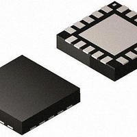
MAX16922ATPA/V+ Maxim Integrated Products, MAX16922ATPA/V+ Datasheet - Page 10

MAX16922ATPA/V+
Manufacturer Part Number
MAX16922ATPA/V+
Description
IC DCDC CONV STPDN DL LDO 20WQFN
Manufacturer
Maxim Integrated Products
Datasheet
1.MAX16922ATPAVT.pdf
(17 pages)
Specifications of MAX16922ATPA/V+
Applications
General Purpose
Current - Supply
5µA
Operating Temperature
-40°C ~ 125°C
Mounting Type
Surface Mount
Package / Case
20-WQFN Exposed Pad, 20-DQFN
Output Voltage
1 V, 2.7 V, 3.3 V, 5 V
Output Current
450 mA, 600 mA, 1.2 A
Switching Frequency
2.2 MHz
Input / Supply Voltage (max)
28 V
Input / Supply Voltage (min)
3.7 V
Maximum Operating Temperature
+ 125 C
Mounting Style
SMD/SMT
Duty Cycle (max)
100 %
Load Regulation
+/- 0.2 %
Minimum Operating Temperature
- 40 C
Number Of Outputs
4
Operating Temperature Range
- 40 C to + 125 C
Supply Current
14 uA
Lead Free Status / RoHS Status
Lead free / RoHS Compliant
Voltage - Supply
-
Lead Free Status / Rohs Status
Lead free / RoHS Compliant
2.2MHz, Dual, Step-Down DC-DC
Converters, Dual LDOs, and RESET
10
TQFN
10
11
12
13
14
15
16
17
18
19
20
______________________________________________________________________________________
—
8
9
PIN
TSSOP
10
11
12
13
14
15
16
17
18
19
20
—
1
2
PGND2
OUTS2
RESET
NAME
GND2
GND1
OUT3
OUT4
LSUP
LX2
PV2
PV3
PV4
EN
EP
OUT2 Voltage Sense Input. Connect OUTS2 directly to the OUT2 output voltage and
bypass to PGND2 with a minimum total capacitance of 10µF. The total capacitance can
include input bypass capacitors cascaded from OUT2, discharged by a 70Ω resistance
between OUTS2 and PGND2 when disabled.
Power Ground for BUCK 2. Connect PGND2 and GND_ together near the device.
Inductor Connection for OUT2. Connect a 2.2µH inductor between LX2 and OUT2 as shown
in the Functional Diagram.
OUT2 Supply Input. Connect a 4.7µF or larger ceramic capacitor from PV2 to ground.
Linear-Regulator Power Input for OUT3. Bypass PV3 to GND with a minimum 2.2µF ceramic
capacitor.
Linear-Regulator 1 Output. Bypass OUT3 to GND with a minimum 2.2µF ceramic capacitor
internally discharged by a 1kΩ resistance when disabled.
Ground. Connect GND, GND1, GND2, and GND3 together.
Linear-Regulator 2 Output. Bypass OUT4 to GND with a minimum 2.2µF ceramic capacitor.
Internally discharged by a 1kΩ resistance when disabled.
Linear-Regulator Power Input for OUT4. Bypass PV4 to GND with a minimum 2.2µF ceramic
capacitor.
5V Logic Supply to Provide Power to Internal Circuitry. Bypass LSUP to GND1 with a 1µF
ceramic capacitor.
Open-Drain Reset Output for the Input Monitoring OUT1 and OUT2. External pullup
required.
Ground. Connect GND, GND1, GND2, and GND3 together.
Active-High Enable Input. Connect EN to PV1 or a logic-high voltage to turn on all
regulators. Pull EN input low to place the regulators in shutdown.
Exposed Pad. Connect the exposed pad to ground. Connecting the exposed pad to ground
does not remove the requirement for proper ground connections to PGND2 and GND_. The
exposed pad is attached with epoxy to the substrate of the die, making it an excellent path
to remove heat from the device.
FUNCTION
Pin Description (continued)


