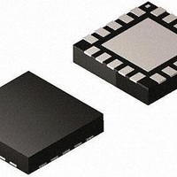
MAX16922ATPA/V+ Maxim Integrated Products, MAX16922ATPA/V+ Datasheet - Page 12

MAX16922ATPA/V+
Manufacturer Part Number
MAX16922ATPA/V+
Description
IC DCDC CONV STPDN DL LDO 20WQFN
Manufacturer
Maxim Integrated Products
Datasheet
1.MAX16922ATPAVT.pdf
(17 pages)
Specifications of MAX16922ATPA/V+
Applications
General Purpose
Current - Supply
5µA
Operating Temperature
-40°C ~ 125°C
Mounting Type
Surface Mount
Package / Case
20-WQFN Exposed Pad, 20-DQFN
Output Voltage
1 V, 2.7 V, 3.3 V, 5 V
Output Current
450 mA, 600 mA, 1.2 A
Switching Frequency
2.2 MHz
Input / Supply Voltage (max)
28 V
Input / Supply Voltage (min)
3.7 V
Maximum Operating Temperature
+ 125 C
Mounting Style
SMD/SMT
Duty Cycle (max)
100 %
Load Regulation
+/- 0.2 %
Minimum Operating Temperature
- 40 C
Number Of Outputs
4
Operating Temperature Range
- 40 C to + 125 C
Supply Current
14 uA
Lead Free Status / RoHS Status
Lead free / RoHS Compliant
Voltage - Supply
-
Lead Free Status / Rohs Status
Lead free / RoHS Compliant
2.2MHz, Dual, Step-Down DC-DC
Converters, Dual LDOs, and RESET
The MAX16922 limits the peak inductor current sourced
by the p-channel MOSFET. When the peak current limit
is reached, the internal p-channel MOSFET turns off for
the remainder of the cycle. If the current limit is exceed-
ed for 16 consecutive cycles, and the output voltage is
less than 1.25V, the p-channel MOSFET is turned off
and enters output discharge mode for 256 clock
cycles, allowing the inductor current and output voltage
to discharge. Once completed, a soft-start sequence is
initiated on OUT2.
As the input voltage approaches the output voltage, the
duty cycle of the p-channel MOSFET reaches 100%. In
this state, the p-channel MOSFET is turned on constant-
ly (not switching), and the dropout voltage is the volt-
age drop due to the output current across the
on-resistance of the internal p-channel MOSFET (R
and the inductor’s DC resistance (R
The MAX16922 operates in either auto-PWM or forced-
PWM modes. At light load, auto-PWM switches only as
needed to supply the load to improve light-load efficiency
of the step-down converter. At higher load currents
(~160mA), the step-down converter transitions to fixed
2.2MHz switching frequency. Forced PWM always oper-
ates with a constant 2.2MHz switching frequency regard-
less of the load. Connect PWM high for forced-PWM
applications or low for auto-PWM applications.
The MAX16922 contains two low-dropout linear regula-
tors (LDOs), OUT3 and OUT4. The LDO output voltages
are factory preset, and each LDO supplies loads up to
300mA. The LDOs include an internal reference, error
amplifier, p-channel pass transistor, and internal volt-
age-dividers. Each error amplifier compares the refer-
ence voltage to the output voltage (divided by the
internal voltage-divider) and amplifies the difference. If
the divided feedback voltage is lower than the refer-
ence voltage, the pass-transistor gate is pulled lower,
allowing more current to pass to the outputs and
increasing the output voltage. If the divided feedback
voltage is too high, the pass-transistor gate is pulled up,
allowing less current to pass to the output. Each output
voltage is factory selectable from 1.0V to 4.15V in 50mV
increments. If not using one of the LDO outputs, then tie
the associated input power pin (PV_) to ground.
12
______________________________________________________________________________________
V
DO
= I
LOAD
LDO Linear Regulators
(R
PCH
+ R
L
):
L
)
Current Limit
Dropout
PWM
PCH
)
An undervoltage-lockout circuit turns off the LDO
regulators when the input supply voltage is too low to
guarantee proper operation. When PV3 falls below
1.25V (typ), OUT3 powers down. When PV4 falls below
1.5V (typ), OUT4 powers down.
OUT3 enters soft-start when PV3 exceeds 1.25V, and
OUT4 enters soft-start when PV4 exceeds 1.5V. This
staggers the surge current during startup to prevent
excess current draw from OUT1 or OUT2 that could
trigger an overcurrent shutdown. The soft-start time for
each LDO is 0.1ms (typ). See the startup waveforms in
the Typical Operating Characteristics section.
The OUT3 and OUT4 output current is limited to 450mA
(typ). If the output current exceeds the current limit, the
corresponding LDO output voltage drops out of regula-
tion. Excess power dissipation in the device can cause
the device to turn off due to thermal shutdown.
The dropout voltage for the linear regulators is 320mV
(max) at 250mA load. To avoid dropout, make sure the
input supply voltage corresponding to OUT3 and OUT4
is greater than the corresponding output voltage plus
the dropout voltage based on the application output
current requirements.
LSUP is the output of a 5V linear regulator that powers
MAX16922 internal circuitry. LSUP is internally powered
from PV1 and automatically powers up when EN is high
and PV1 exceeds approximately 3.7V. LSUP automati-
cally powers down when EN is taken low. Bypass LSUP
to GND with a 1µF ceramic capacitor. LSUP remains on
even during a thermal fault.
Thermal-overload protection limits the total power dissi-
pation in the MAX16922. Thermal-protection circuits
monitor the die temperature. If the die temperature
exceeds +175°C, the device shuts down, allowing it to
cool. Once the device has cooled by 15°C, the device
is enabled again. This results in a pulsed output during
continuous thermal-overload conditions. The thermal-
overload protection protects the MAX16922 in the event
of fault conditions. For continuous operation, do not
exceed the absolute maximum junction temperature of
+150°C. See the Thermal Considerations section for
more information.
Input Supply and Undervoltage Lockout
Thermal-Overload Protection
LSUP Linear Regulator
Current Limit
Soft-Start
Dropout


