TDA3629T/N2,112 NXP Semiconductors, TDA3629T/N2,112 Datasheet - Page 15

TDA3629T/N2,112
Manufacturer Part Number
TDA3629T/N2,112
Description
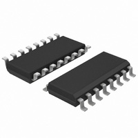
IC LIGHT POSITION CTRLR 16-SOIC
Manufacturer
NXP Semiconductors
Datasheet
1.TDA3629TN2112.pdf
(28 pages)
Specifications of TDA3629T/N2,112
Applications
Automotive
Current - Supply
6mA
Voltage - Supply
8 V ~ 18 V
Operating Temperature
-40°C ~ 105°C
Mounting Type
Surface Mount
Package / Case
16-SOIC (3.9mm Width)
Product
Fan / Motor Controllers / Drivers
Mounting Style
SMD/SMT
Lead Free Status / RoHS Status
Lead free / RoHS Compliant
Other names
935216410112
TDA3629T/N2
TDA3629T/N2
TDA3629T/N2
TDA3629T/N2
Philips Semiconductors
IMMUNITY TO NARROW BAND ELECTROMAGNETIC
DISTURBANCES
Test procedure
G
The immunity is measured using a test procedure, which
is derived from the draft international standard
“ISO/DIS 11452” , parts 1 and 7, submitted for circulation
1992 June 14.
The test is carried out using a printed-circuit test board in
a test set-up, which is illustrated in Fig.13. The circuit
diagram of the test board is shown in Fig.14. The physical
layout of the test board is shown in Figs 15 to 17.
P
The IC under test is mounted onto the printed-circuit test
board. The printed-circuit test board is mounted into the
faraday cage (RF-shielded 19 inch-rack) and connected to
the test equipment as shown in Fig.13. One of three RF
voltage injection points has to be chosen for injection,
while the others have to be connected to passive
terminations. The injection into the control loop via input
RFC is shown in Fig.13.
After the set-up is completed, the feedback voltage is
selected by the appropriate setting of a jumper in the
jumper field J1 (see Fig.14) and the battery voltage is
switched on. With no RF voltage injected the correct
operation of the system is verified by turning the SET
potentiometer (see Fig.13) left and right (or vice-versa).
The outputs OUT1 and OUT2 will switch to on-state
(absolute differential voltage V
turn directions. If the device under test functions correctly,
the potentiometer is set to a position where the absolute
voltage difference between the slider connection of the
potentiometer and the jumper J1 is less than 5 mV.
After adjustment, the absolute differential output voltage
V
condition the immunity test may be started.
T
For the test of immunity the RF voltage is injected into the
test board and V
degraded if its actual value exceeds the maximum value
described in Table 2. In the test routine the frequency is
varied in steps from the start frequency to the stop
frequency (see Table 2). Within each frequency step the
level of injected RF voltage is incremented by steps to the
maximum test level, which is specified in Table 2.
Each step level is held constant for the dwell time. After the
dwell time has elapsed, the degradation of the absolute
output voltage is checked. If a degradation is detected it
1996 Sep 04
EST OF IMMUNITY
REPARATION OF TEST
diff
ENERAL INFORMATION
Light position controller
has to be below 100 mV. Having reached this
diff
is monitored for degradation. V
diff
= 3 to 5 V DC) in both
diff
is
15
has to be verified, because the level setting may have an
overshoot and the device under test may have a latching
behaviour. The verification is achieved by switching off the
power supply for 1 s after degradation is first detected.
Then the supply is switched on and the degradation is
rechecked. If the second check also indicates a
degradation, then the values of RF level and frequency are
inserted into a data file for reporting. If the second check is
negative the level is further increased.
If no degradation occurs until the specified maximum test
level is reached, the maximum level is recorded together
with the frequency of that step.
R
For a fast setting of the RF voltage to the required test level
step it is recommended that the substitution method is
used.
This method sets the actual test level with respect to level
values that have been filed in a pre-measurement.
The RF source in the test set-up is built from a low-power
RF generator and suitable amplifiers. In the recommended
pre-measurement the RF voltage at the injection point is
measured, while the signal generator outputs a constant
voltage level (e.g. 100 mV). Thus, the gain factor from the
output of the RF generator to the injection point can be
easily calculated.
In the pre-measurement the RF voltage at the injection
point is measured for each frequency step. Dividing this
measured voltage by 100 mV results in the gain factor for
this frequency. All gain factors together with their
frequency value are filed for use in the level setting of the
immunity tests.
In the immunity test routine, a required RF voltage test
level at a frequency step is obtained by setting the RF
signal generator to a level that is calculated by dividing the
required RF voltage test level by the gain factor of that
frequency.
Test conditions
The test is carried out using the test procedure as
mentioned before and under the conditions mentioned in
Table 2.
ECOMMENDED
RF-
VOLTAGE SETTING PROCEDURE
Product specification
TDA3629


