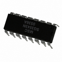
SG3543N Microsemi Analog Mixed Signal Group, SG3543N Datasheet - Page 3

SG3543N
Manufacturer Part Number
SG3543N
Description
IC POWER SUPPLY SUPERVISOR 16DIP
Manufacturer
Microsemi Analog Mixed Signal Group
Datasheet
1.SG3543DW.pdf
(6 pages)
Specifications of SG3543N
Applications
Power Supply, Supervisor
Voltage - Supply
4.5 V ~ 40 V
Current - Supply
7mA
Operating Temperature
0°C ~ 70°C
Mounting Type
Through Hole
Package / Case
16-DIP
Lead Free Status / RoHS Status
Lead free / RoHS Compliant
Voltage - Input
-
Available stocks
Company
Part Number
Manufacturer
Quantity
Price
Rev 1.1a
Copyright
ELECTRICAL CHARACTERISTICS
Note 5. Input voltage rising on O.V. Input and falling on U.V. Input.
CHARACTERISTIC CURVES
Comparator Section
Input Threshold
Input Hysteresis
Input Bias Current
Delay Saturation
Delay High Level
Delay Charging Current
Indicate Saturation
Indicate Leakage
Propagation Delay
SCR Trigger Section
Peak Output Current
Peak Output Voltage
Output Off Voltage
Remote Activate Current
Remote Activate Voltage
Reset Current
Reset Voltage
Output Current Rise Time
Prop. Delay from REM. ACT. Pin
Prop. Delay fom O.V. INPUT Pin
Current Limit Section
Input Voltage Range
Input Bias Current
Input Offset Voltage
CMRR
AVOL
Output Saturation
Output Leakage
Small Signal Bandwidth
Propagation Delay
1994
Parameter
FIGURE 1.
SCR TRIGGER POWER LIMITING
(Note 5)
OFFSET/COMP pin open, V
OFFSET/COMP pin open, V
10k
0
OFFSET/COMP pin open, V
I
V
A
V
T
Sense input = 0V
V
I
V
V
+V
+V
+V
REM. ACT. pin = Gnd
REM. ACT pin open
RESET pin = Gnd, REM. ACT. = Gnd
RESET pin open, REM. ACT. = Gnd
R
L
L
J
IND
V
OVERDRIVE
D
IND
O.V. INPUT
L
= 10mA
= 10mA
C
C
V
V
= 25 C
IN
IN
IN
= 0dB, T
= 0V
= 50 , T
V
REM. ACT.
O.V. INPUT
D
D
= 40V
= 40V
= 5V, R
= 15V, I
= 40V, R
(continued)
CM
= 0
= 1 F
from OFFSET/COMP pin to Gnd,T
= 2.7V, V
12V, V
= 100mV, T
= 0.4V
= 2.7V
J
J
G
O
= 25 C
= 25 C, C
L
= 0, V
= 100mA
= 1K
Test Conditions
IN
U.V. INPUT
= 15V
O
J
= 0
= 25 C
D
= 0
= 2.3V , T
3
CM
CM
CM
= 0V
= 0V,
= 0V
J
= 25 C
FIGURE 2 .
ACTIVATION DELAY VS. CAPACITOR VALUE
J
=25°C
Min. Typ. Max. Min. Typ. Max.
2.45
2.40
200
100
12
80
60
72
SG1543/2543
0
2.50
250
400
200
400
300
500
100
200
0.3
0.2
0.2
.01
0.4
0.4
0.3
0.2
.01
25
10
13
70
80
6
0
2
2
0
5
11861 Western Avenue
V
2.55
2.60
300
400
120
1.0
0.5
0.5
1.0
0.1
0.8
0.8
1.0
0.5
1.0
IN
10
8
6
6
-3V
2.40
2.35
(714) 898-8121
200
100
12
70
60
72
0
SG3543
2.50
250
400
200
400
300
500
100
200
0.3
0.2
0.2
0.1
0.4
0.4
0.3
0.2
.01
25
10
13
70
80
6
0
2
2
0
5
Garden Grove, CA 92841
V
2.60
2.65
300
400
130
1.0
0.5
0.5
1.0
0.1
0.8
0.8
IN
1.0
0.5
1.0
15
FAX: (714) 893-2570
8
6
6
-3V
mA/ s
Units
MHz
mV
mA
mA
mA
mV
mV
ms
dB
dB
ns
ns
ns
ns
V
V
V
V
V
V
V
V
V
V
V
A
A
A
A
A


