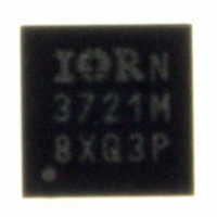
IR3721MTRPBF International Rectifier, IR3721MTRPBF Datasheet - Page 2

IR3721MTRPBF
Manufacturer Part Number
IR3721MTRPBF
Description
IC POWER SUPPLY MONITOR 10-DFN
Manufacturer
International Rectifier
Series
TruePower™r
Datasheet
1.IR3721MTRPBF.pdf
(16 pages)
Specifications of IR3721MTRPBF
Applications
Power Supply Monitor
Voltage - Supply
3.135 V ~ 3.465 V
Current - Supply
350µA
Operating Temperature
0°C ~ 125°C
Mounting Type
Surface Mount
Package / Case
10-DFN
Quiescent Current
450µA
Bandwidth
589kHz
Sensor Case Style
DFN
No. Of Pins
10
Supply Voltage Range
3.135V To 3.465V
Operating Temperature Range
0°C To +125°C
Filter Terminals
SMD
Rohs Compliant
No
Accuracy %
2.5%
Package
10 Lead 3x3 DFN
Static Accuracy
2.5% @ 65oC
Vk Range
0.5V - 1.8V
Vcs Range
5mV - 150mV
Bias Supply Voltage
+3.3V +/-5%
Junction Temperature
0oC to 125oC
Pbf
Yes
Lead Free Status / RoHS Status
Lead free / RoHS Compliant
Voltage - Input
-
Other names
IR3721MTRPBFTR
Available stocks
Company
Part Number
Manufacturer
Quantity
Price
Part Number:
IR3721MTRPBF
Manufacturer:
IR
Quantity:
20 000
ABSOLUTE MAXIMUM RATINGS
Absolute Maximum Ratings (Referenced to GND)
VDD:.................................................................3.9V
All other Analog and Digital pins ......................3.9V
Stresses beyond those listed under “Absolute Maximum Ratings” may cause permanent damage to the device.
These are stress ratings only and functional operation of the device at these or any other conditions beyond those
indicated in the operational sections of the specifications are not implied. Exposure to absolute maximum rating
conditions for extended periods may affect device reliability.
ELECTRICAL SPECIFICATIONS
Unless otherwise specified, these specifications apply: VDD = 3.3V ± 5%, 0
operation in the typical application circuit. See notes following table.
BIAS SUPPLY
VDD Turn-on Threshold, VDD
VDD Turn-off Threshold, VDD
VDD UVLO Hysteresis
VDD Operating Current, ICC
VOLTAGE REFERENCE
V
R
ΔΣ CONVERTER
Vo common mode range
Duty Ratio Accuracy
Duty Ratio Accuracy
Sampling frequency, f
Comparator Offset
CS pin input current, I
DIGITAL OUTPUT
VK pin voltage range
DI source resistance
Page 2 of 16
RT
T
resistance range
Voltage
NOTES:
1.
Guaranteed by design
PARAMETER
CLK
CS
UP
DN
www.irf.com
DI output low when off
R
Note 1
V
R
T
V
R
Note 1
DI output low
j
DCR
DCR
T
T
T
=65°C, Note 1
=25.5kΩ, R
=25.5kΩ, R
= 25.5k Ω
=20 mV, V
=20 mV, V
TEST CONDITION
CS1
CS1
O
O
Operating Junction Temperature .... -10°C to 150°C
Storage Temperature Range .......... -65°C to 150°C
ESD Rating ............HBM Class 2 JEDEC Standard
MSL Rating ..................................................Level 2
Reflow Temperature ..................................... 260°C
=1V,
=1V,
+R
+R
CS2
CS2
=600 Ω
=600 Ω,
o
C ≤ T
J
1.452
1250
-250
MIN
-0.5
≤ 125
435
2.4
0.5
0.5
75
o
C, 0.5 ≤ Vo ≤ 1.8 V, and
1.493
2000
TYP
25.5
350
512
DATA SHEET
1.535
MAX
+250
3000
3.10
+0.5
450
589
1.8
2.5
1.8
IR3721
4
09/15/08
UNIT
kHz
mV
mV
μA
kΩ
nA
%
%
V
V
Ω
V
V
V


