AD636JHZ Analog Devices Inc, AD636JHZ Datasheet

IC CONV RMS-DC LOW LVL TO100-10

AD636JHZ

Manufacturer Part Number
AD636JHZ
Description
IC CONV RMS-DC LOW LVL TO100-10
Manufacturer
Analog Devices Inc
Datasheet

Specifications of AD636JHZ

Current - Supply
800µA
Voltage - Supply
±2.5 V ~ 16 V
Mounting Type
Through Hole
Package / Case
TO-100, Metal Can (10 Leads)
Accuracy %
1%
Bandwidth
130kHz
Supply Current
800µA
Power Dissipation Pd
500mW
Supply Voltage Range
2V, 5V To 24V
Digital Ic Case Style
TO-100
No. Of Pins
10
Lead Free Status / RoHS Status
Lead free / RoHS Compliant

Available stocks

Company
Part Number
Manufacturer
Quantity
Price
Part Number:
AD636JHZ
Manufacturer:
REALTEK
Quantity:
2 760
Part Number:
AD636JHZ
Manufacturer:
ADI
Quantity:
485
FEATURES
True rms-to-dc conversion
200 mV full scale
Laser-trimmed to high accuracy
Wide response capability
dB output with 50 dB range
Low power: 800 μA quiescent current
Single or dual supply operation
Monolithic integrated circuit
Low cost
GENERAL DESCRIPTION
The AD636 is a low power monolithic IC that performs true
rms-to-dc conversion on low level signals. It offers performance
that is comparable or superior to that of hybrid and modular
converters costing much more. The AD636 is specified for a
signal range of 0 mV to 200 mV rms. Crest factors up to 6 can
be accommodated with less than 0.5% additional error, allowing
accurate measurement of complex input waveforms.
The low power supply current requirement of the AD636,
typically 800 μA, is ideal for battery-powered portable
instruments. It operates from a wide range of dual and single
power supplies, from ±2.5 V to ±16.5 V or from +5 V to +24 V.
The input and output terminals are fully protected; the input
signal can exceed the power supply with no damage to the device
(allowing the presence of input signals in the absence of supply
voltage), and the output buffer amplifier is short-circuit protected.
The AD636 includes an auxiliary dB output derived from an
internal circuit point that represents the logarithm of the rms
output. The 0 dB reference level is set by an externally supplied
current and can be selected to correspond to any input level from
0 dBm (774.6 mV) to −20 dBm (77.46 mV). Frequency response
ranges from 1.2 MHz at 0 dBm to greater than 10 kHz at −50 dBm.
The AD636 is easy to use. The device is factory-trimmed at the
wafer level for input and output offset, positive and negative
waveform symmetry (dc reversal error), and full-scale accuracy
Rev. D
Information furnished by Analog Devices is believed to be accurate and reliable. However, no
responsibility is assumed by Analog Devices for its use, nor for any infringements of patents or other
rights of third parties that may result from its use. Specifications subject to change without notice. No
license is granted by implication or otherwise under any patent or patent rights of Analog Devices.
Trademarks and registered trademarks are the property of their respective owners.
0.5% maximum error (AD636K)
1.0% maximum error (AD636J)
Computes rms of ac and dc signals
1 MHz, −3 dB bandwidth: V rms > 100 mV
Signal crest factor of 6 for 0.5% error
Low Level, True RMS-to-DC Converter
One Technology Way, P.O. Box 9106, Norwood, MA 02062-9106, U.S.A.
Tel: 781.329.4700
Fax: 781.461.3113
at 200 mV rms. Therefore, no external trims are required to
achieve full-rated accuracy.
The AD636 is available in two accuracy grades. The total error
of the J-version is typically less than ±0.5 mV ± 1.0% of reading,
while the total error of the AD636K is less than ±0.2 mV to
±0.5% of reading. Both versions are temperature rated for
operation between 0°C and 70°C and available in 14-lead
SBDIP and 10-lead TO-100 metal can.
The AD636 computes the true root-mean-square of a complex
ac (or ac plus dc) input signal and gives an equivalent dc output
level. The true rms value of a waveform is a more useful
quantity than the average rectified value because it is a measure
of the power in the signal. The rms value of an ac-coupled
signal is also its standard deviation.
The 200 mV full-scale range of the AD636 is compatible with
many popular display-oriented ADCs. The low power supply
current requirement permits use in battery-powered hand-held
instruments. An averaging capacitor is the only external
component required to perform measurements to the fully
specified accuracy is. Its value optimizes the trade-off between
low frequency accuracy, ripple, and settling time.
An optional on-chip amplifier acts as a buffer for the input or
the output signals. Used in the input, it provides accurate
performance from standard 10 MΩ input attenuators. As an
output buffer, it sources up to 5 mA.
+V
S
BUF IN
C
V
AV
IN
FUNCTIONAL BLOCK DIAGRAM
ABSOLUTE
AD636
VALUE
©2006 Analog Devices, Inc. All rights reserved.
Figure 1.
10kΩ
SQUARER
CURRENT
DIVIDER
MIRROR
10kΩ
www.analog.com
AD636
dB
R
I
BUF OUT
OUT
L

Related parts for AD636JHZ

AD636JHZ Summary of contents

Page 1

FEATURES True rms-to-dc conversion 200 mV full scale Laser-trimmed to high accuracy 0.5% maximum error (AD636K) 1.0% maximum error (AD636J) Wide response capability Computes rms of ac and dc signals 1 MHz, −3 dB bandwidth: V rms > 100 mV ...

Page 2

AD636 TABLE OF CONTENTS Features .............................................................................................. 1 Functional Block Diagram .............................................................. 1 General Description ......................................................................... 1 Revision History ............................................................................... 2 Specifications..................................................................................... 3 Absolute Maximum Ratings............................................................ 5 ESD Caution.................................................................................. 5 Pin Configurations and Function Descriptions ........................... 6 Applying the AD636......................................................................... 7 ...

Page 3

SPECIFICATIONS @ 25° and −V = –5 V, unless otherwise noted Table 1. Model TRANSFER FUNCTION CONVERSION ACCURACY 2, 3 Total Error, Internal Trim vs. Temperature, 0°C to +70°C vs. Supply Voltage DC Reversal ...

Page 4

AD636 Model dB OUTPUT Error 300 mV rms IN Scale Factor Scale Factor Temperature Coefficient I for 0.1 V rms REF I Range REF I TERMINAL OUT I Scale Factor OUT I ...

Page 5

ABSOLUTE MAXIMUM RATINGS Table 2. Parameter Supply Voltage Dual Supply Single Supply 1 Internal Power Dissipation Maximum Input Voltage Storage Temperature Range Operating Temperature Range Lead Temperature Range (Soldering 60 sec) ESD Rating 1 10-Lead TO: θ = 150°C/W. JA ...

Page 6

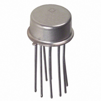
AD636 PIN CONFIGURATIONS AND FUNCTION DESCRIPTIONS –V AD636 TOP VIEW (Not to Scale BUF OUT 6 BUF CONNECT ...

Page 7

APPLYING THE AD636 The input and output signal ranges are a function of the supply voltages as detailed in the specifications. The AD636 can also be used in an unbuffered voltage output mode by disconnecting the input to the buffer. ...

Page 8

AD636 C AV – 3.3µ ABSOLUTE VALUE NONPOLARIZED NC 2 AD636 – SQUARER DIVIDER CURRENT dB 5 MIRROR V OUT BUF OUT 6 10kΩ BUF IN ...

Page 9

The 2-pole post filter uses an active filter stage to provide even greater ripple reduction without substantially increasing the settling times over a circuit with a 1-pole filter. The values C2, and C3 can then be reduced ...

Page 10

AD636 swing, this configuration allows the output to swing fully down to ground in single-supply applications without the problems associated with most IC operational amplifiers CURRENT MIRROR 5µA 5µA 10kΩ BUFFER INPUT R E 40kΩ R –V EXTERNAL ...

Page 11

A COMPLETE AC DIGITAL VOLTMETER Figure 17 shows a design for a complete low power ac digital voltmeter circuit based on the AD636. The 10 MΩ input attenuator allows full-scale ranges of 200 mV and 200 ...

Page 12

AD636 D1 1N4148 + R5 C4 – 47kΩ 2.2µ 200mV 10% 1MΩ 0.02µF 9MΩ 900kΩ – 20V + 6.8µF R3 90kΩ BUF OUT 200V BUF IN R4 10kΩ R7 20kΩ COM D4 ...

Page 13

... AD636JD 0°C to +70°C 1 AD636JDZ 0°C to +70°C AD636KD 0°C to +70°C 1 AD636KDZ 0°C to +70°C AD636JH 0°C to +70°C 1 AD636JHZ 0°C to +70°C AD636KH 0°C to +70°C 1 AD636KHZ 0°C to +70° Pb-free part. 0.005 (0.13) MIN 0.080 (2.03) MAX 14 8 0.310 (7.87) ...

Page 14

AD636 NOTES Rev Page ...

Page 15

NOTES Rev Page AD636 ...

Page 16

AD636 NOTES ©2006 Analog Devices, Inc. All rights reserved. Trademarks and registered trademarks are the property of their respective owners. C00787-0-11/06(D) Rev Page ...

Related keywords