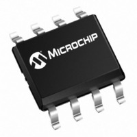
TC72-5.0MUA Microchip Technology, TC72-5.0MUA Datasheet - Page 10

TC72-5.0MUA
Manufacturer Part Number
TC72-5.0MUA
Description
SENSOR THERMAL SPI 5.0V 8MSOP
Manufacturer
Microchip Technology
Datasheet
1.TC72-5.0MUA.pdf
(24 pages)
Specifications of TC72-5.0MUA
Function
Temp Monitoring System (Sensor)
Topology
ADC (Sigma Delta), Register Bank
Sensor Type
Internal
Sensing Temperature
-55°C ~ 125°C
Output Type
SPI™
Output Alarm
No
Output Fan
No
Voltage - Supply
2.65 V ~ 5.5 V
Operating Temperature
-55°C ~ 125°C
Mounting Type
Surface Mount
Package / Case
8-MSOP, Micro8™, 8-uMAX, 8-uSOP,
Ic Output Type
Digital
Sensing Accuracy Range
± 2°C
Supply Current
400µA
Supply Voltage Range
2.65V To 5.5V
Resolution (bits)
10bit
Sensor Case Style
MSOP
No. Of Pins
8
Full Temp Accuracy
3 C
Digital Output - Bus Interface
SPI
Digital Output - Number Of Bits
10 bit
Supply Voltage (max)
5.5 V
Supply Voltage (min)
2.6 V
Description/function
High Accuracy 10-bit Serial Output, 4-Wire SPI Interface
Maximum Operating Temperature
+ 125 C
Minimum Operating Temperature
- 55 C
Temperature Sensing Range
-55°C To +125°C
Rohs Compliant
Yes
Lead Free Status / RoHS Status
Lead free / RoHS Compliant
For Use With
TC72DM-PICTL - BOARD DEMO PICTAIL TC72
Lead Free Status / Rohs Status
Lead free / RoHS Compliant
Available stocks
Company
Part Number
Manufacturer
Quantity
Price
Company:
Part Number:
TC72-5.0MUA
Manufacturer:
Microchip Technology
Quantity:
390
Part Number:
TC72-5.0MUA
Manufacturer:
MICROCHIP/微芯
Quantity:
20 000
TC72
TABLE 3-3:
3.4
The temperature and control register data is outputted
from the TC72 using the CE, SCK and SDO lines.
Figure 3-3 shows a timing diagram of the read opera-
tion. Communication is initiated by the chip enable (CE)
going high. The SDO line remains at the voltage level
of the LSb bit that is outputted and goes to the tri-state
level when the CE line goes to a logic low level.
3.5
Data is clocked into the Control register in order to
enable the TC72’s power saving shutdown mode. The
write operation is shown in Figure 3-3 and is
accomplished using the CE, SCK and SDI line.
DS21743A-page 10
Write (A7 = 1)
Read (A7 = 0)
Note 1: CP is the Clock Polarity of the microcontroller system clock. If the inactive state of SCK is logic level high,
Disable
Mode
2: During a Read operation, SDO remains at a high impedance (High Z) level until the eight bits of data begin
Read Operation
Write Operation
CP is equal to ‘1’; otherwise, if the inactive state of SCK is low, CP is equal to ‘0’.
to be shifted out of the Temperature register.
OPERATIONAL MODES
CE
H
H
L
CP=1, Data Shifted on Falling Edge,
Data Clocked on Rising Edge
CP=0, Data Shifted on Rising Edge,
Data Clocked on Falling Edge
CP=1, Data Shifted on Falling Edge,
Data Clocked on Rising Edge
CP=0, Data Shifted on Rising Edge,
Data Clocked on Falling Edge
Input Disabled
SCK (Note 1)
FIGURE 3-2:
Operation.
CP = 0
CP = 1
SCK
SCK
CE
CE
Input Disabled
Data Bit Latch
SDI
X
SHIFT
EDGE
SHIFT
EDGE
Serial Clock Polarity (CP)
2002 Microchip Technology Inc.
CLOCK
EDGE
CLOCK
Next data bit shift,
EDGE
Note 2
High Z
High Z
SDO


