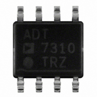
ADT7310TRZ Analog Devices Inc, ADT7310TRZ Datasheet - Page 18

ADT7310TRZ
Manufacturer Part Number
ADT7310TRZ
Description
IC TEMP SENSOR 16BIT SPI 8SOIC
Manufacturer
Analog Devices Inc
Datasheet
1.ADT7310TRZ.pdf
(24 pages)
Specifications of ADT7310TRZ
Function
Temp Monitoring System (Sensor)
Topology
ADC (Sigma Delta), Oscillator, Register Bank
Sensor Type
Internal
Sensing Temperature
-55°C ~ 150°C
Output Type
SPI™
Output Alarm
Yes
Output Fan
No
Voltage - Supply
2.7 V ~ 5.5 V
Operating Temperature
-55°C ~ 150°C
Mounting Type
Surface Mount
Package / Case
8-SOIC (3.9mm Width)
Ic Output Type
Digital
Sensing Accuracy Range
± 0.5°C
Supply Current
230µA
Supply Voltage Range
2.7V To 5.5V
Resolution (bits)
16bit
Sensor Case Style
SOIC
No. Of Pins
8
Temperature Sensor Function
Temp Sensor
Package Type
SOIC N
Operating Temperature (max)
150C
Operating Temperature Classification
Military
Operating Supply Voltage (min)
2.7V
Operating Supply Voltage (typ)
3.3/5V
Operating Supply Voltage (max)
5.5V
Lead Free Status / RoHS Status
Lead free / RoHS Compliant
Lead Free Status / RoHS Status
Lead free / RoHS Compliant, Lead free / RoHS Compliant
Available stocks
Company
Part Number
Manufacturer
Quantity
Price
Company:
Part Number:
ADT7310TRZ-REEL7
Manufacturer:
AD
Quantity:
2 100
ADT7310
SERIAL INTERFACE
The ADT7310 has a 4-wire serial peripheral interface (SPI). The
interface has a data input pin (DIN) for inputting data to the
device, a data output pin (DOUT) for reading data back from
the device, and a data clock pin (SCLK) for clocking data into
and out of the device. A chip select pin ( CS ) enables or disables
the serial interface. CS is required for correct operation of the
interface. Data is clocked out of the ADT7310 on the negative
edge of SCLK, and data is clocked into the device on the
positive edge of SCLK.
SPI COMMAND BYTE
All data transactions on the bus begin with the master taking
CS from high to low and sending out the command byte. This
indicates to the ADT7310 whether the transaction is a read or
a write and provides the address of the register for the data
transfer.
Table 15. Command Byte
C7
0
C6
R/W
Table 15
C5
Register address
shows the command byte.
C4
C3
C2
Continuous
read
MICROCONTROLLER
Figure 17. Typical SPI Interface Connection
C1
0
C0
0
Rev. 0 | Page 18 of 24
SCLK
DOUT
DIN
CS
ADT7310
GND
Bit C7 of the command byte must be set to 0 to successfully
begin a bus transaction. The SPI interface does not work
correctly if a 1 is written into this bit.
Bit C6 is the read/write bit; 1 indicates a read, and 0 indicates
a write.
Bits[C5:C3] contain the target register address. One register can
be read from or written to per bus transaction.
Bit C2 activates a continuous read mode on the temperature
value register only. When this bit is set, the serial interface is
configured so that the temperature value register can be
continuously read. When the command word is 01010100
(0x54), the contents of the temperature value register can be
read out without requiring repeated writes to set the address
bits. Simply sending 16 SCLK clocks to the ADT7310 clocks the
contents of the temperature value register onto the DOUT pin.
V
INT
CT
DD
V
DD
0.1µF
PULL-UP
10kΩ
V
DD
10kΩ


