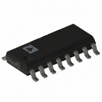
AD7417ARZ Analog Devices Inc, AD7417ARZ Datasheet

AD7417ARZ
Specifications of AD7417ARZ
Available stocks
Related parts for AD7417ARZ
AD7417ARZ Summary of contents
Page 1
FEATURES 10-bit ADC with 15 μs and 30 μs conversion times Single and 4 single-ended analog input channels On-chip temperature sensor: −40°C to +125°C On-chip track-and-hold Overtemperature indicator Automatic power-down at the end of a conversion Wide operating supply range: ...
Page 2
AD7416/AD7417/AD7418 TABLE OF CONTENTS Features .............................................................................................. 1 Applications....................................................................................... 1 General Description ......................................................................... 1 Functional Block Diagrams............................................................. 1 Revision History ............................................................................... 2 Product Highlights ........................................................................... 3 Specifications..................................................................................... 4 AD7417/AD7418 Specifications................................................. 4 AD7416 Specifications................................................................. 6 Absolute Maximum Ratings............................................................ 7 ESD Caution.................................................................................. 7 ...
Page 3
An I C® compatible serial interface allows the AD7416/AD7417/ AD7418 registers to be written to and read back. The three LSBs of the AD7416/AD7417 serial bus address can be selected, which allows up to eight AD7416/AD7417 devices to be ...
Page 4
AD7416/AD7417/AD7418 SPECIFICATIONS AD7417/AD7418 SPECIFICATIONS 5.5 V, GND = 0 V, REF DD IN Table 1. Parameter DC ACCURACY Resolution Minimum Resolution for Which No Missing Codes Are Guaranteed 2 Relative Accuracy 2 Differential Nonlinearity 2 ...
Page 5
Parameter POWER REQUIREMENTS Normal Operation Power-Down Auto Power-Down Mode 10 SPS Throughput Rate 1 kSPS Throughput Rate 10 kSPS Throughput Rate Power-Down 1 B Version applies to AD7417 only with temperature range of −40°C to +85°C. ...
Page 6
AD7416/AD7417/AD7418 AD7416 SPECIFICATIONS 5.5 V, GND = 0 V, REF DD IN Table 2. Parameter TEMPERATURE SENSOR AND ADC Accuracy Resolution Temperature Conversion Time Update Rate OTI Delay Supply Current T Default Temperature ...
Page 7
ABSOLUTE MAXIMUM RATINGS T = 25°C, unless otherwise noted. A Table 3. Parameter V to AGND DGND DD Analog Input Voltage to AGND IN1 IN4 1 Reference Input Voltage to AGND Digital Input Voltage ...
Page 8
AD7416/AD7417/AD7418 PIN CONFIGURATIONS AND FUNCTION DESCRIPTIONS Table 4. AD7417 Pin Function Descriptions Pin No. Mnemonic Description Connection. Do not connect anything to this pin. 2 SDA Digital I/O. Serial bus bidirectional data. Push-pull output. 3 SCL ...
Page 9
SDA 1 AD7416 SCL 2 OTI 3 TOP VIEW (Not to Scale) GND 4 Figure 7. AD7416 Pin Configuration (SOIC/MSOP) Table 5. AD7416 Pin Function Descriptions Pin No. Mnemonic Description 1 SDA Digital I/O. Serial bus bidirectional data. Push-pull output. ...
Page 10
AD7416/AD7417/AD7418 TERMINOLOGY Relative Accuracy Relative accuracy or endpoint nonlinearity is the maximum deviation from a straight line passing through the endpoints of the ADC transfer function. Differential Nonlinearity This is the difference between the measured and the ideal 1 LSB ...
Page 11
THEORY OF OPERATION CIRCUIT INFORMATION The AD7417 and AD7418 are single-channel and four-channel, 15 μs conversion time, 10-bit ADCs with on-chip temperature sensor, reference, and serial interface logic functions on a single chip. The AD7416 has no analog input channel ...
Page 12
AD7416/AD7417/AD7418 An external 2.5 V reference can be connected to the REF This has the effect of shutting down the on-chip reference circuitry. REF IN 1.2V SW1 1.2V 26kΩ 24kΩ Figure 11. On-Chip Reference TEMPERATURE MEASUREMENT A common method of ...
Page 13
Table 8. Register Addresses Registers Temperature value Configuration register setpoint HYST setpoint OTI ADC value (AD7417/AD7418 only ...
Page 14
AD7416/AD7417/AD7418 111...111 111...110 111...000 1LSB – VREF/1024 011...111 000...010 000...001 000...000 0V 1/2LSB +VREF – 1LSB ANALOG INPUT Figure 14. Ideal Transfer Function Characteristic for the AD7417/AD7418 Config2 Register (Address 0x05) A second configuration register is included in the AD7417/ ...
Page 15
This is illustrated in Figure 16. • Writing two bytes of data to the T OTI setpoint register. If 9-bit resolution is required for the temperature setpoints, two bytes of data must be written ...
Page 16
AD7416/AD7417/AD7418 Reading Data From the AD7416/AD7417/AD7418 Reading data from the AD7416/AD7417/AD7418 is a single- byte or 2-byte operation. Reading back the contents of the configuration register is a single-byte read operation, as shown in Figure 18, with the register address ...
Page 17
OTI OUTPUT The OTI output has two operating modes that are selected by Bit D1 of the configuration register. In the comparator mode, (D1 = 0), the OTI output becomes active when the temperature exceeds T and remains active until ...
Page 18
AD7416/AD7417/AD7418 Mode 2 For applications where temperature measurements are required at a slower rate, for example, every second, power consumption of the part can be reduced by writing to the part full power-down between reads. The ...
Page 19
APPLICATIONS INFORMATION SUPPLY DECOUPLING The AD7416/AD7417/AD7418 should be decoupled with a 0.1 μF ceramic capacitor between V and GND. This is DD particularly important if the part is mounted remote from the power supply. POWER-ON RESET To ensure proper power-on ...
Page 20
AD7416/AD7417/AD7418 SYSTEM WITH MULTIPLE AD7416 DEVICES The three LSBs of the AD7416 serial address can be set by the user, allowing eight different addresses from 1001000 to 1001111. Figure 25 shows a system in which eight AD7416 devices are connected ...
Page 21
OUTLINE DIMENSIONS 4.00 (0.1575) 3.80 (0.1496) 0.25 (0.0098) 0.10 (0.0039) COPLANARITY 0.10 0.25 (0.0098) 0.10 (0.0040) COPLANARITY 10.00 (0.3937) 9.80 (0.3858 6.20 (0.2441) 1 5.80 (0.2283) 8 1.27 (0.0500) BSC 1.75 (0.0689) 1.35 (0.0531) SEATING 0.51 (0.0201) 0.25 ...
Page 22
AD7416/AD7417/AD7418 0.15 0.05 5.10 5.00 4. 4.50 6.40 4.40 BSC 4. PIN 1 1.20 MAX 0.20 0.09 8° 0.30 0.65 0° 0.19 SEATING BSC PLANE COPLANARITY 0.10 COMPLIANT TO JEDEC STANDARDS MO-153-AB Figure 28. 16-Lead Thin ...
Page 23
... AD7417AR-REEL −40°C to +125°C AD7417AR-REEL7 −40°C to +125°C AD7417ARZ −40°C to +125°C AD7417ARZ-REEL −40°C to +125°C AD7417ARZ-REEL7 −40°C to +125°C AD7417ARU −40°C to +125°C AD7417ARU-REEL −40°C to +125°C AD7417ARU-REEL7 −40°C to +125°C AD7417ARUZ − ...
Page 24
AD7416/AD7417/AD7418 NOTES refers to a communications protocol originally developed by Philips Semiconductors (Now NXP Semiconductors). ©1998–2010 Analog Devices, Inc. All rights reserved. Trademarks and registered trademarks are the property of their respective owners. D01126-0-11/10(I) Rev ...


