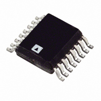
ADT7517ARQZ Analog Devices Inc, ADT7517ARQZ Datasheet - Page 40

ADT7517ARQZ
Manufacturer Part Number
ADT7517ARQZ
Description
IC SENSOR TEMP QD ADC/DAC 16QSOP
Manufacturer
Analog Devices Inc
Datasheet
1.ADT7517ARQZ.pdf
(44 pages)
Specifications of ADT7517ARQZ
Function
Temp Monitoring System (Sensor)
Topology
ADC, Comparator, Multiplexer, Register Bank
Sensor Type
External & Internal
Sensing Temperature
-40°C ~ 120°C, External Sensor
Output Type
I²C™, MICROWIRE™, QSPI™, SPI™
Output Alarm
No
Output Fan
No
Voltage - Supply
2.7 V ~ 5.5 V
Operating Temperature
-40°C ~ 120°C
Mounting Type
Surface Mount
Package / Case
16-QSOP
Ic Output Type
Voltage
Sensing Accuracy Range
± 0.5°C
Supply Current
2.2mA
Supply Voltage Range
2.7V To 5.5V
Resolution (bits)
10bit
Sensor Case Style
QSOP
No. Of Pins
16
Temperature Sensor Function
Temp Sensor
Resolution
10b
Operating Temperature (min)
-40C
Operating Temperature (max)
120C
Operating Supply Voltage (min)
2.7V
Operating Supply Voltage (typ)
3.3/5V
Operating Supply Voltage (max)
5.5V
Lead Free Status / RoHS Status
Lead free / RoHS Compliant
Lead Free Status / RoHS Status
Lead free / RoHS Compliant, Lead free / RoHS Compliant
Available stocks
Company
Part Number
Manufacturer
Quantity
Price
Company:
Part Number:
ADT7517ARQZ
Manufacturer:
Analog Devices Inc
Quantity:
135
ADT7516/ADT7517/ADT7519
Write Operation
Figure 63 shows the timing diagram for a write operation to the
ADT7516/ADT7517/ADT7519. Data is clocked into the
registers on the rising edge of SCLK. When the CS line is high,
the DIN and DOUT lines are in three-state mode. Only when
the CS goes from a high to a low does the part accept any data
on the DIN line. In SPI mode, the address pointer register is
capable of auto-incrementing to the next register in the register
map without having to load the address pointer register each
time. In Figure 63, the register address portion gives the first
register that is written to. Subsequent data bytes are written into
sequential writable registers. Thus, after each data byte has been
written into a register, the address pointer register auto-
increments its value to the next available register. The address
pointer register auto-increments from 0x00 to 0x3F and loops
back to start again at 0x00 when it reaches 0x3F.
SCLK
DIN
CS
START
Figure 63. SPI—Writing to the Address Pointer Register Followed by a Single Byte of Data to the Selected Register
D7
1
D6
WRITE COMMAND
D5
D4
SCLK (CONTINUED)
DIN (CONTINUED)
D3
CS (CONTINUED)
D2
D1
Rev. B | Page 40 of 44
D0
8
D7
D7
1
1
Read Operation
Figure 64 to Figure 66 show the timing diagrams necessary to
accomplish correct read operations. To read back from a
register, first write to the address pointer register with the
address of the register to be read from. This operation is shown
in Figure 64. Figure 65 shows the procedure for reading back a
single byte of data. The read command is first sent to the part
during the first eight clock cycles. As the read command is
being sent, irrelevant data is output onto the DOUT line.
During the following eight clock cycles, the data contained in
the register selected by the address pointer register is output
onto the DOUT line. Data is output onto the DOUT line on the
falling edge of SCLK. Figure 66 shows the procedure when
reading data from two sequential registers. Multiple data reads
are possible in the SPI interface mode as the address pointer
register is auto-incremental. The address pointer register auto-
increments from 0x00 to 0x3F and loops back to start again at
0x00 when it reaches 0x3F.
D6
D6
REGISTER ADDRESS
D5
D5
DATA BYTE
D4
D4
D3
D3
D2
D2
D1
D1
D0
D0
STOP
8
8


