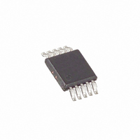
MAX6683AUB+ Maxim Integrated Products, MAX6683AUB+ Datasheet - Page 11

MAX6683AUB+
Manufacturer Part Number
MAX6683AUB+
Description
IC TEMP SENSOR MON 10-UMAX
Manufacturer
Maxim Integrated Products
Datasheet
1.MAX6683AUBT.pdf
(14 pages)
Specifications of MAX6683AUB+
Function
Temp Monitoring System (Sensor)
Topology
ADC, Multiplexer, Register Bank
Sensor Type
Internal
Sensing Temperature
-40°C ~ 125°C
Output Type
I²C™/SMBus™
Output Alarm
Yes
Output Fan
No
Voltage - Supply
2.7 V ~ 5.5 V
Operating Temperature
-40°C ~ 125°C
Mounting Type
Surface Mount
Package / Case
10-MSOP, Micro10™, 10-uMAX, 10-uSOP
Full Temp Accuracy
+/- 3 C
Digital Output - Bus Interface
Serial (2-Wire)
Digital Output - Number Of Bits
10 bit + Sign
Maximum Operating Temperature
+ 125 C
Minimum Operating Temperature
- 40 C
Lead Free Status / RoHS Status
Lead free / RoHS Compliant
Figure 3. SMBus Write Timing Diagram
Figure 4. SMBus Read Timing Diagram
From a software prospective, the MAX6683 appears as
a set of byte-wide registers that contain voltage and tem-
perature data, alarm threshold values, or control bits.
The device employs five standard SMBus protocols:
write byte, read byte, read word, send byte, and
receive byte (Figures 2, 3, 4).
The device address can be set to one of four different
values by pin strapping ADD to GND, SDA, SCL, or
SMBus/I
SMBCLK
SMBDATA
SMBCLK
SMBDATA
A = START CONDITION
B = MSB OF ADDRESS CLOCKED INTO SLAVE
C = LSB OF ADDRESS CLOCKED INTO SLAVE
D = R/W BIT CLOCKED INTO SLAVE
E = SLAVE PULLS SMBDATA LINE LOW
A = START CONDITION
B = MSB OF ADDRESS CLOCKED INTO SLAVE
C = LSB OF ADDRESS CLOCKED INTO SLAVE
D = R/W BIT CLOCKED INTO SLAVE
t
SU:STA
t
SU:STA
2
C-Compatible Digital Interface
A
A
______________________________________________________________________________________
t
HD:STA
t
HD:STA
t
LOW
t
LOW
B
B
t
HIGH
t
HIGH
System Monitor in a 10-Pin µMAX
t
SU:DAT
t
Slave Address
SU:DAT
C
C
F = ACKNOWLEDGE BIT CLOCKED INTO MASTER
G = MSB OF DATA CLOCKED INTO SLAVE
H = LSB OF DATA CLOCKED INTO SLAVE
I = SLAVE PULLS SMBDATA LINE LOW
E = SLAVE PULLS SMBDATA LINE LOW
F = ACKNOWLEDGE BIT CLOCKED INTO MASTER
G = MSB OF DATA CLOCKED INTO MASTER
H = LSB OF DATA CLOCKED INTO MASTER
I = MASTER PULLS DATA LINE LOW
D
D
E
E
Temperature Sensor and
F
F
V
same bus without address conflicts (Table 1). The
address pin state is checked at the beginning of each
SMBus/I
V
Serial Address Register and overwrites the code set by
connecting the ADD pin until the MAX6683 is taken
through a POR cycle.
The MAX6683 also responds to the SMBus alert
response address (see Alert Response Address).
CC
CC
t
HD:DAT
, so more than one MAX6683 can reside on the
. Any address code can also be written to the
G
G
2
C transaction and is insensitive to glitches on
H
H
J = ACKNOWLEDGE CLOCKED INTO SLAVE
K = ACKNOWLEDGE CLOCK PULSE
L = STOP CONDITION
M = NEW START CONDITION
J = ACKNOWLEDGE CLOCKED INTO MASTER
K = ACKNOWLEDGE CLOCK PULSE
L = STOP CONDITION, DATA EXECUTED BY SLAVE
M = NEW START CONDITION
I
I
J
J
K
K
t
SU:STO
t
SU:STO
L
L
t
BUF
t
BUF
M
M
11


