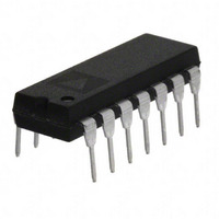
AD650JNZ Analog Devices Inc, AD650JNZ Datasheet - Page 4

AD650JNZ
Manufacturer Part Number
AD650JNZ
Description
IC V-F/F-V CONVERTER 14-DIP
Manufacturer
Analog Devices Inc
Type
Volt to Freq & Freq to Voltr
Datasheet
1.AD650KNZ.pdf
(20 pages)
Specifications of AD650JNZ
Mounting Type
Through Hole
Frequency - Max
1MHz
Full Scale
±150ppm/°C
Linearity
±0.1%
Package / Case
14-DIP (0.300", 7.62mm)
Frequency
1MHz
Full Scale Range
1MHz
Linearity %
0.02%
Supply Voltage Range
± 9V To ± 18V
Digital Ic Case Style
DIP
No. Of Pins
14
Ic Generic Number
650
Converter Function
VFC/FVC
Full Scale Frequency
1000
Power Supply Requirement
Dual
Single Supply Voltage (typ)
Not RequiredV
Single Supply Voltage (max)
Not RequiredV
Single Supply Voltage (min)
Not RequiredV
Dual Supply Voltage (min)
±9V
Dual Supply Voltage (max)
±18V
Operating Temperature (min)
0C
Operating Temperature (max)
70C
Operating Temperature Classification
Commercial
Package Type
PDIP
Calibration Error Fs Typ
5%
Rohs Compliant
Yes
Lead Free Status / RoHS Status
Lead free / RoHS Compliant
Lead Free Status / RoHS Status
Lead free / RoHS Compliant, Lead free / RoHS Compliant
Available stocks
Company
Part Number
Manufacturer
Quantity
Price
Company:
Part Number:
AD650JNZ
Manufacturer:
AD
Quantity:
1 000
Company:
Part Number:
AD650JNZ
Manufacturer:
LINEAR
Quantity:
7 838
Part Number:
AD650JNZ
Manufacturer:
ADI/亚德诺
Quantity:
20 000
AD650
Model
AMPLIFIER OUTPUT (F/V CONVERSION)
POWER SUPPLY
TEMPERATURE RANGE
1
2
3
4
5
Specifications shown in boldface are tested on all production units at final electrical test. Results from those tests are used to calculate outgoing quality levels. All min
Nonlinearity is defined as deviation from a straight line from zero to full scale, expressed as a fraction of full scale.
Full-scale calibration error adjustable to zero.
Measured at full-scale output frequency of 100 kHz.
Refer to F/V conversion section of the text.
Referred to digital ground.
and max specifications are guaranteed, although only those shown in boldface are tested on all production units.
Voltage Range
Source Current
Capacitive Load
Voltage, Rated Performance
Quiescent Current
Rated Performance
(1500 Ω Min Load Resistance)
(750 Ω Max Load Resistance)
(Without Oscillation)
N Package
D Package
Min
0
10
±9
0
−25
AD650J/AD650A
Typ
Max
10
100
±18
8
+70
+85
Rev. D | Page 4 of 20
Min
0
10
±9
0
−25
AD650K/AD650B
Typ
Max
10
100
±18
8
+70
+85
Min
0
10
±9
−55
Typ
AD650S
Max
10
100
±18
8
+125
Units
V
mA
pF
V
mA
°C
°C


