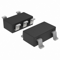
NCP100SNT1G ON Semiconductor, NCP100SNT1G Datasheet - Page 8

NCP100SNT1G
Manufacturer Part Number
NCP100SNT1G
Description
IC REG SHUNT PREC ADJ 1V SOT23-5
Manufacturer
ON Semiconductor
Datasheet
1.NCP100SNT1G.pdf
(12 pages)
Specifications of NCP100SNT1G
Reference Type
Shunt, Adjustable
Voltage - Output
0.9 ~ 6 V
Tolerance
±2.6%
Number Of Channels
1
Current - Cathode
80µA
Current - Output
20mA
Operating Temperature
-40°C ~ 85°C
Mounting Type
Surface Mount
Package / Case
TSOT-23-5, TSOT-5, TSOP-5
Product
Voltage References
Topology
Shunt References
Output Voltage
0.9 V to 6 V
Initial Accuracy
1.7 %
Series Vref - Input Voltage (max)
7 V
Shunt Current (max)
20 mA
Maximum Operating Temperature
+ 85 C
Input Voltage
1 mV
Minimum Operating Temperature
- 40 C
Mounting Style
SMD/SMT
Shunt Current (min)
0.1 mA
Fixed / Adjust / Prog
Adjust
Output Voltage (max)
0.9 to 6V
Reference Voltage Accuracy (max)
1.7
Input Voltage (max)
7V
Operating Temp Range
-40C to 85C
Operating Temperature Classification
Industrial
Mounting
Surface Mount
Pin Count
5
Package Type
TSOP
Lead Free Status / RoHS Status
Lead free / RoHS Compliant
Voltage - Input
-
Temperature Coefficient
-
Current - Quiescent
-
Lead Free Status / Rohs Status
Lead free / RoHS Compliant
Other names
NCP100SNT1GOS
NCP100SNT1GOS
NCP100SNT1GOSTR
NCP100SNT1GOS
NCP100SNT1GOSTR
Available stocks
Company
Part Number
Manufacturer
Quantity
Price
Company:
Part Number:
NCP100SNT1G
Manufacturer:
ON Semiconductor
Quantity:
138 584
Part Number:
NCP100SNT1G
Manufacturer:
ON/安森美
Quantity:
20 000
the exception of the effects of R
voltage across R
voltage slightly down since the R1/R2 voltage divider will
try to hold the point it is connected to at the programmed
voltage. The regulator V
value of the V
NCP100’s intrinsic positive impedance versus cathode
current (I
impedance.
Figure 23. Cathode Current vs. Cathode Voltage for
The circuit performs the same as the one in Figure 21 with
V
5.0
comp
20
15
10
0.94
0
effectively adjusts the NCP100 programmed V
R
K
0.15
comp
(W)
1.5
3.1
) to allow for 0 W or even a negative dynamic
0
R
0.95
comp
comp
Programmed V
comp
|Z
V
−1.4
−1.6
(W)
V comp + I KA R comp
0.2
= 3.1 W
KA
0
KA
. This effect can compensate for the
0.96
, CATHODE VOLTAGE (V)
|
also increases by:
I
T
Figure 22
K
A
= 0.1 mA to 20 mA
KA
= 25° C
0.97
will now be lowered by the
−1.0
−2.0
−3.0
KA
3.0
2.0
1.0
comp
0
= 1.5 W
0.98
0
= 1.0 V
R
. As I
V
comp
Figure 25. Dynamic Impedance vs. Cathode
KA
= 0.15 W
= 1.0 V
0.99
, CATHODE COMPENSATION RESISTANCE (W)
K
= 0 W
1.0
increases, the
Compensation Resistance
= 3.3 V
1.00
http://onsemi.com
= 6.0 V
2.0
KA
1.01
8
of 1.0 V. The NCP100 intrinsic positive dynamic impedance
response is the R
impedance regulator response is realized with R
0.15 W. Negative dynamic impedance responses are
achieved with R
of 6.0 V. The 0 W dynamic impedance value corresponds to
R
compensation resistance for programmed voltages of 1.0 V,
3.3 V and 6.0 V. It can be seen that any value up to the
positive intrinsic dynamic impedance of the NCP100 can be
realized. The other limit is that with a high enough negative
dynamic impedance, the NCP100 V may drop below the
minimum operating V
in unpredictable performance.
3.0
comp
Figure 24. Cathode Current vs. Cathode Voltage for
5.0
Figure 23 shows this phenomenon for a program voltage
Figure 24 shows the characteristic at a programmed V
Figure 25 shows the dynamic impedance versus cathode
I
f ≤1.0 kHz
Figure 22
T
20
15
10
K
5.94
A
0
= 1.0 mA to 20 mA
= 25° C
= 2.9 W.
R
I
T
Figure 22
K
comp
A
= 0.1 to 20 mA
= 25° C
4.0
5.96
= 5.8 W
V
Programmed V
comp
KA
, CATHODE VOLTAGE (V)
comp
5.98
u 0.15 W.
5.0
KA
= 4.4 W
= 0 W curve. A 0 W dynamic
voltage of 0.9 V, which can result
6.00
KA
= 2.9 W
= 6.0 V
6.02
= 1.5 W
R
comp
1.5
2.9
4.4
5.8
W
6.04
0
= 0 W
comp
|Z
−1.6
−2.9
2.9
1.4
W
0
KA
6.06
|
KA
=


