VRE3025AS Cirrus Logic Inc, VRE3025AS Datasheet
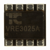
IC VOLT REF PREC 2.5V 8-SMD

VRE3025AS

Manufacturer Part Number
VRE3025AS
Description
IC VOLT REF PREC 2.5V 8-SMD
Manufacturer
Cirrus Logic Inc
Datasheet

Specifications of VRE3025AS

Reference Type
Series
Voltage - Output
2.5V
Tolerance
±0.25mV
Temperature Coefficient
0.6ppm/°C
Voltage - Input
8 ~ 36 V
Number Of Channels
1
Current - Quiescent
4mA
Current - Output
15mA
Operating Temperature
0°C ~ 70°C
Mounting Type
Surface Mount
Package / Case
8-SMD
Product
Voltage References
Topology
Series References
Output Voltage
2.5 V
Average Temperature Coefficient (typ)
0.6 PPM / C
Series Vref - Input Voltage (max)
40 V
Shunt Current (max)
15 mA
Maximum Operating Temperature
+ 70 C
Minimum Operating Temperature
0 C
Mounting Style
Through Hole
Lead Free Status / RoHS Status
Lead free / RoHS Compliant
Current - Cathode
-
Lead Free Status / Rohs Status
Lead free / RoHS Compliant
Other names
598-1773
FEATURES
♦ +2.5 V Output, ± 0.25 mV (.01%)
♦ Temperature Drift: 0.6 ppm/ºc
♦ Low Noise: 1.5 μV
♦ Low Thermal Hysteresis: 1 ppm Typical
♦ ±15 mA Output Source and Sink Current
♦ Excellent Line Regulation: 5 ppm/V Typical
♦ Optional Noise Reduction and Voltage Trim
♦ Industry Standard Pinout: 8-pin DIP or
APPLICATIONS
The VRE3025 is recommended for use as a refer-
ence for 14, 16, or 18 bit data converters which re-
quire an external precision reference. The device
is also ideal for calibrating scale factor on high
resolution data converters. The VRE3025 offers
superior performance over monolithic references.
VRE3025DS
SELECTION GUIDE
VRE3025AS
VRE3025AD
VRE3025BS
VRE3025BD
VRE3025CS
VRE3025CD
VRE3025JS
VRE3025JD
VRE3025KS
VRE3025LS
Surface Mount Package
Model
www.cirrus.com
Initial
Error
0.250
0.250
0.375
0.375
0.500
0.500
0.250
0.250
0.375
0.500
(mV)
®
P r o d u c t T e c h n o l o g y F r o m
P r o d u c t I n n o v a t i o n F r o m
VRE3025
P-P
(ppm/ºC)
Precision Voltage Reference
Temp.
Coeff.
(0.1Hz-10Hz)
0.6
0.6
1.0
1.0
2.0
2.0
0.6
0.6
1.0
2.0
-40ºC to +85ºC
-40ºC to +85ºC
-40ºC to +85ºC
-40ºC to +85ºC
Temp. Range
0ºC to +70ºC
0ºC to +70ºC
0ºC to +70ºC
0ºC to +70ºC
0ºC to +70ºC
0ºC to +70ºC
Figure 1. BLOCK DIAGRAM
(ºC)
Copyright © Cirrus Logic, Inc. 2010
R1
R2
8
(All Rights Reserved)
SMT8 (GF)
SMT8 (GF)
SMT8 (GF)
SMT8 (GF)
SMT8 (GF)
SMT8 (GF)
DIP8 (KD)
DIP8 (KD)
DIP8 (KD)
DIP8 (KD)
Package
Options
4
R3
DESCRIPTION
The VRE3025 is a low cost, high precision +2.5 V ref-
erence that operates from +10 V. The device features
a buried zener for low noise and excellent long term
stability. Packaged in either an 8-pin DIP or SMT op-
tion, the device is ideal for high resolution data conver-
sion systems.
The device provides ultrastable +2.5 V output with
±0.25 mV (.01%) initial accuracy and a temperature
coefficient of 0.6 ppm/ºC. This improvement in accu-
racy is made possible by a unique, patented multipoint
laser compensation technique. Significant improve-
ments have been made in other performance param-
eters as well, including initial accuracy, warm-up drift,
line regulation, and long-term stability, making the
VRE3025 series the most accurate reference avail-
able.
For enhanced performance, the VRE3025 has an ex-
ternal trim option for users who want less than 0.01%
initial error. For ultra low noise applications, an exter-
nal capacitor can be attached between the noise re-
duction pin and the ground pin.
R4
+
-
8-pin Surface Mount
Package Style GF
2
5
6
APEX − VRE3025DSREVH
VRE3025
Package Style KD
VRE3025
8-pin DIP
SEP 2010
1

Related parts for VRE3025AS

VRE3025AS Summary of contents

Page 1

... The device is also ideal for calibrating scale factor on high resolution data converters. The VRE3025 offers superior performance over monolithic references. SELECTION GUIDE Initial Temp. Error Coeff. Model (mV) (ppm/ºC) VRE3025AS 0.250 0.6 VRE3025AD 0.250 0.6 VRE3025BS 0.375 1.0 VRE3025BD 0.375 1.0 VRE3025CS 0 ...

Page 2

VRE3025 1. CHARACTERISTICS AND SPECIFICATIONS ABSOLUTE MAXIMUM RATINGS Power Supply ........................... -0.3V to +40V OUT, TRIM ................................ -0.3V to +12V NR .............................................. -0.3V to +6V Operating Temp. (A,B,C) ........... 0ºC to +70ºC Operating Temp. (J,L) ............. -40ºC to +85ºC ELECTRICAL ...

Page 3

TYPICAL PERFORMANCE CURVES V vs. TEMPERATURE OUT 1.00 0.75 0.50 Upp er Li mit Up per Lim it ...

Page 4

VRE3025 OUTPUT NOISE-VOLTAGE DENSITY vs. FREQUENCY 100 1k 10k Frequency (Hz) 3. THEORY OF OPERATION The following discussion refers to the block diagram in Figure 1. A FET current source is used to bias ...

Page 5

EXTERNAL CONNECTIONS + Optional Noise 8 Reduction Capacitor VRE3025 C 1µ PIN DESCRIPTIONS 1, ...

Page 6

VRE3025 10000 1000 100 10 1 0.1 0.01 1 Reference TC vs. ∆T change from 25°C for 1 LSB change 6. THERMAL HYSTERISIS A change in output voltage as a result of a temperature change. When references experience a temperature ...

Related keywords