AD581KH Analog Devices Inc, AD581KH Datasheet
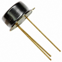
IC PREC VOLT REF 10V TO-5-3

AD581KH

Manufacturer Part Number
AD581KH
Description
IC PREC VOLT REF 10V TO-5-3
Manufacturer
Analog Devices Inc
Type
Voltage Referencer
Datasheets

Specifications of AD581KH

Temperature Coefficient
15ppm/°C
Reference Type
Series
Voltage - Output
10V
Tolerance
±10mV
Voltage - Input
12 ~ 30 V
Number Of Channels
1
Current - Quiescent
1mA
Current - Output
10mA
Operating Temperature
0°C ~ 70°C
Mounting Type
Through Hole
Package / Case
TO-5-3, Metal Can
Topology
Series
Input Voltage
12V To 30V
Reference Voltage
10V
Reference Voltage Tolerance
10mV
No. Of Pins
3
Operating Temperature Range
0°C To +70°C
Current, Output
10 mA
Current, Quiescent Supply
0.75 mA (Typ.) @ 25 °C
Current, Short Circuit
30 mA (Typ.) @ 25 °C
Current, Supply
0.75 mA
Load Regulation
200 uV⁄mA (Typ.) @ 25 °C
Package Type
TO-5
Power Dissipation
600 mW
Regulation, Line
3 mV
Regulation, Load
200 μV/mA
Standards
MIL-STD-883
Temperature, Operating, Maximum
150 °C
Temperature, Operating, Minimum
-65 °C
Temperature, Operating, Range
-65 to +150 °C
Voltage, Input
15 V
Voltage, Noise
40 μVp-p
Voltage, Output
±6.5 (Max.) @ 25 °C
Voltage, Supply
12 to 30 V
Low Quiescent Current
1.0 mA max
Lead Free Status / RoHS Status
Lead free / RoHS Compliant
Current - Cathode
-
Lead Free Status / Rohs Status
RoHS Compliant part Electrostatic Device

Available stocks

Company
Part Number
Manufacturer
Quantity
Price
Part Number:
AD581KH
Manufacturer:
AD
Quantity:
5 530
Part Number:
AD581KH
Manufacturer:
AD
Quantity:
5 530
Part Number:
AD581KH
Manufacturer:
ADI
Quantity:
431
Part Number:
AD581KH
Manufacturer:
ADI/亚德诺
Quantity:
20 000
FEATURES
Laser trimmed to high accuracy
Trimmed temperature coefficient
Excellent long-term stability
−10 V reference capability
Low quiescent current: 1.0 mA maximum
10 mA current output capability
3-pin TO-5 package
MIL-STD-883 compliant versions available
GENERAL DESCRIPTION
The AD581 is a 3-pin, temperature compensated, monolithic,
band gap voltage reference that provides a precise 10.00 V output
from an unregulated input level ranging from 12 V to 30 V.
Laser wafer trimming (LWT) is used to trim both the initial
error at +25°C as well as the temperature coefficient, resulting
in high precision performance previously available only in expen-
sive hybrids or oven regulated modules. The 5 mV initial error
tolerance and 5 ppm/°C guaranteed temperature coefficient of
the AD581L is available in a monolithic voltage reference.
The band gap circuit design used in the AD581 offers several
advantages over classical Zener breakdown diode techniques.
Most important, no external components are required to
achieve full accuracy and significant stability to low power
systems. In addition, total supply current to the device,
including the output buffer amplifier (which can supply up
to 10 mA) is typically 750 μA. The long-term stability of the
band gap design is equivalent to selected Zener reference
diodes.
The AD581 is recommended for use as a reference for 8-, 10-
or 12-bit digital-to-analog converters (DACs) that require an
external precision reference. The device is also ideal for all types
of analog-to-digital converters (ADCs) up to 14-bit accuracy,
either successive approximation or integrating designs, and can
generally offer better performance than that provided by standard
self-contained references.
Rev. C
Information furnished by Analog Devices is believed to be accurate and reliable. However, no
responsibility is assumed by Analog Devices for its use, nor for any infringements of patents or other
rights of third parties that may result from its use. Specifications subject to change without notice. No
license is granted by implication or otherwise under any patent or patent rights of Analog Devices.
Trademarks and registered trademarks are the property of their respective owners.
10.000 V ±5 mV (L and U models)
5 ppm/°C maximum, 0°C to 70°C (L model)
10 ppm/°C maximum, −55°C to +125°C (U model)
25 ppm/1000 hrs (noncumulative)
One Technology Way, P.O. Box 9106, Norwood, MA 02062-9106, U.S.A.
Tel: 781.329.4700
Fax: 781.461.3113
The AD581J, AD581K, and AD581L are specified for operation
from 0°C to 70°C; the AD581S, AD581T, and AD581U are
specified for the −55°C to +125°C range. All grades are
packaged in a hermetically sealed 3-pin TO-5 metal can.
PRODUCT HIGHLIGHTS
1.
2.
3.
4.
5.
Laser trimming of both initial accuracy and temperature
coefficient results in very low errors over temperature
without the use of external components. The AD581L has
a maximum deviation from 10.000 V of ±7.25 mV from
0°C to 70°C, whereas the AD581U guarantees ±15 mV
maximum total error without external trims from −55°C
to +125°C.
Because the laser trimming is done on the wafer prior to
separation into individual chips, the AD581 is extremely
valuable to hybrid designers for its ease of use, lack of
required external trims, and inherent high performance.
The AD581 can also be operated in a 2-pin Zener mode to
provide a precision −10 V reference with just one external
resistor to the unregulated supply. The performance in this
mode is nearly equal to that of the standard 3-pin confi-
guration.
Advanced circuit design using the band gap concept allows
the AD581 to give full performance with an unregulated
input voltage down to 13 V. With an external resistor, the
device operates with a supply as low as 11.4 V.
The AD581 is available in versions compliant with
MILSTD-883. Refer to the military datasheet for detailed
specifications.
FUNCTIONAL BLOCK DIAGRAM
AD581
©2009 Analog Devices, Inc. All rights reserved.
BOTTOM VIEW
10 V IC Reference
Figure 1.
TO-5
GND
+V
S
High Precision
V
OUT
www.analog.com
AD581

Related parts for AD581KH

AD581KH Summary of contents

Page 1

FEATURES Laser trimmed to high accuracy 10.000 V ± and U models) Trimmed temperature coefficient 5 ppm/°C maximum, 0°C to 70°C (L model) 10 ppm/°C maximum, −55°C to +125°C (U model) Excellent long-term stability 25 ppm/1000 hrs (noncumulative) ...

Page 2

AD581 TABLE OF CONTENTS Features .............................................................................................. 1 Functional Block Diagram .............................................................. 1 General Description ......................................................................... 1 Product Highlights ........................................................................... 1 Revision History ............................................................................... 2 Specifications ..................................................................................... 3 Absolute Maximum Ratings ............................................................ 5 ESD Caution .................................................................................. 5 Applying the AD581 ......................................................................... ...

Page 3

... AD581JH AD581KH Rev Page AD581L Max Min Typ Max Units ±10 ± ±6.75 ±2. ppm/°C 3.0 3.0 mV (0.002) (0.002) %/V 1.0 1.0 mV (0.005) (0.005) %/V 500 ...

Page 4

AD581 Table 2. Model OUTPUT VOLTAGE TOLERANCE (Error from Nominal 10,000 V Output) OUTPUT VOLTAGE CHANGE Maximum Deviation from +25°C Value MIN MAX Temperature Coefficient LINE REGULATION 15 V ≤ V ≤ ...

Page 5

ABSOLUTE MAXIMUM RATINGS Table 3. Parameter Input Voltage Power Dissipation @ +25°C Operating Junction Temperature Range Lead Temperature (Soldering 10 sec) Thermal Resistance Junction-to-Ambient Stresses above those listed under Absolute Maximum Ratings may cause permanent damage to the device. This ...

Page 6

AD581 APPLYING THE AD581 The AD581 is easy to use in virtually all precision reference applications. The three pins are simply: primary supply, ground, and output, with the case grounded. No external components are required even for high precision applications; ...

Page 7

The error band which is guaranteed with the AD581 is the maximum deviation from the initial value at +25°C; this error band is of more use to a designer than one which simply guarantees the maximum total change over the ...

Page 8

AD581 PRECISION HIGH CURRENT SUPPLY The AD581 can be easily connected with power pnp or power Darlington pnp devices to provide much greater output current capability. The circuit shown in Figure 10 delivers a precision 10 V output with up ...

Page 9

THE AD581 AS A CURRENT LIMITER The AD581 represents an alternative to current limiter diodes that require factory selection to achieve a desired current. This approach often results in temperature coefficients of 1%/°C. The AD581 approach is not limited to ...

Page 10

AD581 10 V reference guarantees a maximum full-scale temperature coefficient of 8 ppm/°C over the commercial range. The 10 V reference also supplies the normal 1 mA bipolar offset current through the 9.95 kΩ bipolar offset resistor. Consequently, the bipolar ...

Page 11

... OUTLINE DIMENSIONS 0.030 (0.76) MAX ORDERING GUIDE Model Temperature Range AD581JH 1 0°C to +70°C 1 AD581KH 0°C to +70°C 1 AD581LH 0°C to +70°C 1 AD581SH −55°C to +125°C 1 AD581TH −55°C to +125°C 1 AD581UH −55°C to +125°C 1 RoHS compliant model as of Date Code 0713. ...

Page 12

AD581 NOTES ©2009 Analog Devices, Inc. All rights reserved. Trademarks and registered trademarks are the property of their respective owners. D08014-0-4/09(C) Rev Page ...

Related keywords