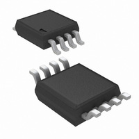
LP2975AIMM-3.3/NOPB National Semiconductor, LP2975AIMM-3.3/NOPB Datasheet - Page 11

LP2975AIMM-3.3/NOPB
Manufacturer Part Number
LP2975AIMM-3.3/NOPB
Description
IC DVR/CTRLR MOSFET LDO 8-MSOP
Manufacturer
National Semiconductor
Type
Positive Fixedr
Datasheet
1.LP2975IMM-5.0NOPB.pdf
(20 pages)
Specifications of LP2975AIMM-3.3/NOPB
Number Of Outputs
1
Voltage - Output
3.3V
Current - Supply
180µA
Voltage - Input
1.8 ~ 24 V
Operating Temperature
-40°C ~ 125°C
Package / Case
8-MSOP, Micro8™, 8-uMAX, 8-uSOP,
Lead Free Status / RoHS Status
Lead free / RoHS Compliant
Other names
LP2975AIMM-3.3
LP2975AIMM-3.3TR
LP2975AIMM-3.3TR
Reference Designs
DESIGN #3: V
Application Circuits, Adjustable Voltage Regulator)
Components
C
C
C
R1 = 261Ω, 1%
R2 = 1.21 kΩ, 1%
R
P-FET = NDP6020P
Heatsink: (Assuming V
against a continuous short-circuit is required, a heatsink with
θ
short-circuit survivability is not needed, a heatsink with θ
Performance Data
Dropout Voltage
Dropout voltage is defined as the minimum input-to-output
differential voltage required by the regulator to keep the
output in regulation. It is measured by reducing V
output voltage drops below the nominal value (the nominal
value is the output voltage measured with V
6A for this test.
Load Regulation
Load regulation is defined as the maximum change in output
voltage as the load current is varied. It is measured by
changing the load resistance and recording the minimum/
maximum output voltage. The measured change in output
voltage is divided by the nominal output voltage and ex-
pressed as a percentage. V
Line Regulation
Line regulation is defined as the maximum change in output
voltage as the input voltage is varied. It is measured by
changing the input voltage and recording the minimum/
maximum output voltage. The measured change in output
voltage is divided by the nominal output voltage and ex-
pressed as a percentage. I
Output Noise Voltage
Output noise voltage was measured by connecting a wide-
band AC voltmeter (HP 400E) directly across the output
capacitor. V
Transient Response
Transient response is defined as the change in output volt-
age which occurs after the load current is suddenly changed.
V
The load resistor is connected to the regulator output using a
switch so that the load current increases from 0 to 6A
abruptly. The change in output voltage is shown in the scope
photo (the vertical scale is 50 mV/division and the horizontal
<
S-A
IN
IN
OUT
C
SC
7 ˚C/W is adequate.
= NOT USED
= 3.3V for this test.
= 1000 µF Aluminum Electrolytic
= 6 mΩ
<
3.3V ≤ V
= 4 X 330 µF OSCON Aluminum Electrolytic
0 ≤ I
2.5 ˚C/W must be used. However, if continuous
IN
L
≤ 6A: LOAD REGULATION = 0.092%
DROPOUT VOLTAGE = 0.68V
= 3.3V and I
IN
OUT
≤ 5V: LINE REGULATION = 0.033%
NOISE = 60 µV (rms)
= 1.5V
IN
≤ 3.3V and T
@
L
L
IN
= 6A for this test.
= 6A for this test.
6A. (Refer to Typical
= 3.3V for this test.
(Continued)
A
≤ 60˚C) if protection
IN
= 3.3V). I
IN
until the
L
S-A
=
11
scale is 20 µs/division. The regulator nominal output (1.5V)
is located on the center line of the photo. A maximum change
of about −80 mV is shown.
Application Hints
SELECTING THE FET
The best choice of FET for a specific application will depend
on a number of factors:
VOLTAGE RATING: The FET must have a Drain-to-Source
breakdown voltage (sometimes called BV
greater than the input voltage.
DRAIN CURRENT: On-state Drain current must be specified
to be greater than the worst-case (short circuit) load current
for the application.
TURN-ON THRESHOLD: The Gate-to-Source voltage
where the FET turns on (called the Gate Threshold Voltage)
is very important. Many FET’s are intended for use with
G-to-S voltages in the 5V to 10V range. These should only
be used in applications where the input voltage is high
enough to provide
Newer FET’s are becoming available with lower turn-on
thresholds (Logic-Level FET’s) which turn on fully with a gate
voltage of only 3V to 4V. Low threshold FET’s should be
used in applications where the input voltage is ≤ 5V.
ON RESISTANCE: FET on resistance (often called R
is a critical parameter since it directly determines the mini-
mum input-to-output voltage required for operation at a given
load current (also called dropout voltage).
R
Source voltage applied. For example, the R
with V
V
dent, increasing at higher temperatures.
The dropout voltage of any LDO design is directly related to
R
Where R
Application Circuit).
GATE CAPACITANCE: Selecting a FET with the lowest
possible Gate capacitance improves LDO performance in
two ways:
G-S
DS
DS
ON is highly dependent on the amount of Gate-to-
ON, as given by:
is increased to 10V. R
G-S
Transient Response for 0–6A Load Step
SC
= 5V will typically decrease by about 25% as the
V
is the short-circuit current limit set resistor (see
DROPOUT
>
5V of drive to the Gate.
= I
LOAD
DS
ON is also temperature depen-
x (R
DS
ON + R
DS
DSS
SC
ON of a FET
)
www.national.com
) which is
DS
10003441
ON)


