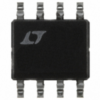
LT1573CS8 Linear Technology, LT1573CS8 Datasheet - Page 12

LT1573CS8
Manufacturer Part Number
LT1573CS8
Description
IC LDO REGULATOR DVR ADJ 8-SOIC
Manufacturer
Linear Technology
Type
Positive Adjustabler
Datasheet
1.LT1573CS8.pdf
(16 pages)
Specifications of LT1573CS8
Number Of Outputs
1
Voltage - Output
1.27 ~ 6.8 V
Current - Supply
1.7mA
Voltage - Input
2.8 ~ 10 V
Operating Temperature
0°C ~ 125°C
Package / Case
8-SOIC (3.9mm Width)
Lead Free Status / RoHS Status
Contains lead / RoHS non-compliant
Available stocks
Company
Part Number
Manufacturer
Quantity
Price
Company:
Part Number:
LT1573CS8
Manufacturer:
Linear Technology
Quantity:
135
Company:
Part Number:
LT1573CS8
Manufacturer:
LT
Quantity:
2 368
Part Number:
LT1573CS8
Manufacturer:
LT/凌特
Quantity:
20 000
Company:
Part Number:
LT1573CS8#PBF
Manufacturer:
LT
Quantity:
1 604
Part Number:
LT1573CS8#PBF
Manufacturer:
LINEAR/凌特
Quantity:
20 000
Company:
Part Number:
LT1573CS8#TR
Manufacturer:
NS
Quantity:
86
Company:
Part Number:
LT1573CS8#TRPBF
Manufacturer:
LINEAR
Quantity:
8 031
Part Number:
LT1573CS8#TRPBF
Manufacturer:
LINEAR/凌特
Quantity:
20 000
Part Number:
LT1573CS8-2.5
Manufacturer:
LINEAR/凌特
Quantity:
20 000
Part Number:
LT1573CS8-2.5#PBF
Manufacturer:
LINEAR/凌特
Quantity:
20 000
APPLICATIO S I FOR ATIO
LT1573
needed during output transients, more capacitance can be
added to the regulator output. If more capacitance is
added to the output, the bandwidth of the regulator is
lowered. A large value compensation capacitor may be
needed to lower the frequency of the compensation zero to
avoid high frequency oscillation. Equal value output
capacitors with different ESR can have different output
transient response. High frequency performance will be
strongly affected by parasitics in the output capacitor and
board layout. Some experimentation with the external
compensation will be required for optimum results.
Shutdown Function
The regulator can be shut down by pulling the SHDN pin
voltage higher than the shutdown threshold (about 1.3V).
The regulator will restart itself if the SHDN is pulled below
the shutdown threshold.The SHDN pin should be tied to
ground if it is not used. The SHDN pin voltage can be
higher than the input voltage. When the SHDN pin voltage
is higher than 2V, the SHDN pin current increases and is
limited by a 20k resistor. Momentarily putting the device
into shutdown also resets the overcurrent latch.
12
U
C
TIME
V
IN
U
+
Figure 3. Reduced Dropout Voltage or Increased Output Current
by Paralleling Output PNP Transistors
FB
LATCH
SHDN
GND
W
LT1573
DRIVE
COMP
V
OUT
V
IN
U
C
IN
C
C
R
R
B1
D1
Lower Dropout Voltage or Higher Output
Current Capability
Lower dropout voltage or higher output current capability
can be achieved by paralleling several output PNP transis-
tors as shown in Figure 3. By paralleling output PNP
transistors, the equivalent resistance between the emit-
ters (V
transistor sharing the output current now runs at a lower
collector current, which causes the dropout voltage to
decrease. Because the PNP transistors are running at a
lower collector current where the transistor beta is higher,
much more output current can be obtained at a given base
drive current. When paralleling two or more output tran-
sistors, a separate resistor is needed for R
each output transistor. This allows the base drive current
to be split evenly between output transistors, which pro-
motes equal output current sharing. In the specific
example drawn in Figure 3 with two output transistors, the
resistance of R
resistance of R
R
In case of n PNP transistors in parallel, the resistance R
Q
D2
OUT1
R
C
is twice the value of the resistance of R
C
OUT1
IN
R
R
D2
B2
) and collectors (V
+
Q
OUT2
B
B1
in Figure 2, and the resistance of R
and R
R1
R2
B2
LOAD
is now twice the value of the
OUT
1573 F03
) is lowered or each PNP
GND
V
OUT
D
B
in Figure 2.
and R
D1
D
and
for
B


