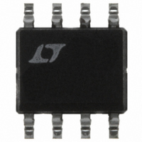
LT1573CS8 Linear Technology, LT1573CS8 Datasheet - Page 8

LT1573CS8
Manufacturer Part Number
LT1573CS8
Description
IC LDO REGULATOR DVR ADJ 8-SOIC
Manufacturer
Linear Technology
Type
Positive Adjustabler
Datasheet
1.LT1573CS8.pdf
(16 pages)
Specifications of LT1573CS8
Number Of Outputs
1
Voltage - Output
1.27 ~ 6.8 V
Current - Supply
1.7mA
Voltage - Input
2.8 ~ 10 V
Operating Temperature
0°C ~ 125°C
Package / Case
8-SOIC (3.9mm Width)
Lead Free Status / RoHS Status
Contains lead / RoHS non-compliant
Available stocks
Company
Part Number
Manufacturer
Quantity
Price
Company:
Part Number:
LT1573CS8
Manufacturer:
Linear Technology
Quantity:
135
Company:
Part Number:
LT1573CS8
Manufacturer:
LT
Quantity:
2 368
Part Number:
LT1573CS8
Manufacturer:
LT/凌特
Quantity:
20 000
Company:
Part Number:
LT1573CS8#PBF
Manufacturer:
LT
Quantity:
1 604
Part Number:
LT1573CS8#PBF
Manufacturer:
LINEAR/凌特
Quantity:
20 000
Company:
Part Number:
LT1573CS8#TR
Manufacturer:
NS
Quantity:
86
Company:
Part Number:
LT1573CS8#TRPBF
Manufacturer:
LINEAR
Quantity:
8 031
Part Number:
LT1573CS8#TRPBF
Manufacturer:
LINEAR/凌特
Quantity:
20 000
Part Number:
LT1573CS8-2.5
Manufacturer:
LINEAR/凌特
Quantity:
20 000
Part Number:
LT1573CS8-2.5#PBF
Manufacturer:
LINEAR/凌特
Quantity:
20 000
APPLICATIO S I FOR ATIO
LT1573
output current with dropout voltage as low as 0.35V. The
gain-bandwidth product f
40MHz which enables the regulator, composed of this
PNP transistor and the LT1573, to handle the load changes
of several amps in a few hundred nanoseconds with a
minimum amount of output capacitance.
The following sections describe how specifications can be
determined for the basic regulator based on the LT1573
and D45H11 from Motorola. To determine the specifica-
tions for regulators formed by the LT1573 and other PNP
transistors, a similar method can be used.
Dropout Voltage
The dropout voltage of an LT1573-based regulator circuit
is determined by the V
external PNP transistor when it is driven with a base
current equal to the available drive current of the LT1573.
The LT1573 is guaranteed to sink 250mA of base current
(440mA typ). The available drive current of the LT1573 can
be reduced by adding a resistor (R
with the DRIVE pin. Table 1 lists some useful operating
points for the D45H11. These points were empirically
determined using a sampling of devices.
Table 1. D45H11 Dropout Voltage
8
DRIVE CURRENT
(mA)
100
100
150
200
150
200
250
20
20
40
40
60
60
80
OUTPUT CURRENT
U
CE
saturation voltage of the discrete
(A)
U
1
2
2
3
3
4
4
4
5
5
5
6
6
7
T
of the D45H11 is typically
D
W
in Figure 2) in series
DROPOUT VOLTAGE
TYPICAL
0.20
0.50
0.25
0.50
0.25
0.70
0.45
0.35
0.70
0.40
0.35
0.65
0.45
0.50
(V)
U
Current Limit
For regulator circuits using the LT1573, current limiting is
achieved by limiting the base drive current to the external
PNP pass transistor. This means that the actual system
current limit will be a function of both the current limit of
the LT1573 and the Beta of the external PNP. Motorola
provides the following Beta information for the D45H11.
The minimum Beta of the D45H11 is 60 when V
I
4A. For other PNP transistors, the user should first find out
the Beta information from the external PNP transistor
manufacturer to determine the appropriate LT1573 base
drive current limit. The current limit of the regulator
system then can be achieved by selecting the appropriate
amount of resistance R
Selecting R
Resistor R
to the external PNP transistor. In order to select R
user should first choose the value of the drive current that
will give the required value of output current and dropout
voltage. For a circuit using the D45H11 as a pass transistor
this can be done using Table 1. For circuits using transis-
tors other than D45H11, the user must characterize the
transistor to determine the drive current requirements for
the specified output current and dropout voltage. In gen-
eral, it is recommended that the user choose the lowest
value of drive current that will satisfy the output current
requirements. This will minimize the stress on circuit
components during overload conditions.
The formula used to determine the resistor R
where,
V
V
I
I
V
C
DRIVE
RB
IN
BE
DRIVE
= 2A. The minimum Beta is 40 when V
R
= the current through R
= the minimum input voltage to the circuit
= the maximum emitter/base voltage of the PNP
D
= (V
pass transistor
pin current equals (I
= the minimum PNP base current required
= the DRIVE pin saturation voltage when the DRIVE
D
IN
D
can be used to limit the available drive current
– V
BE
– V
DRIVE
D
in Figure 2.
DRIVE
)/(I
B
= V
DRIVE
+ I
BE
/R
RB
+ I
B
)
RB
CE
)
= 1V and I
D
CE
is:
= 1V and
D
, the
C
(1)
=


