SG3525AN Microsemi Analog Mixed Signal Group, SG3525AN Datasheet
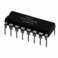
IC PWM POWER SUPPLY SW 16DIP

SG3525AN

Manufacturer Part Number
SG3525AN
Description
IC PWM POWER SUPPLY SW 16DIP
Manufacturer
Microsemi Analog Mixed Signal Group
Datasheet

Specifications of SG3525AN

Pwm Type
Voltage Mode
Number Of Outputs
2
Frequency - Max
350kHz
Duty Cycle
49%
Voltage - Supply
8 V ~ 35 V
Buck
Yes
Boost
No
Flyback
No
Inverting
No
Doubler
No
Divider
No
Cuk
No
Isolated
No
Operating Temperature
0°C ~ 70°C
Package / Case
16-DIP
Frequency-max
350kHz
Lead Free Status / RoHS Status
Lead free / RoHS Compliant

Available stocks

Company
Part Number
Manufacturer
Quantity
Price
Part Number:
SG3525AN
Manufacturer:
MOTOROLA
Quantity:
53
Part Number:
SG3525AN
Manufacturer:
ON
Quantity:
5 510
Part Number:
SG3525AN
Manufacturer:
ST-MICROELECTRONICS
Quantity:
2 442
Part Number:
SG3525AN
Manufacturer:
STM
Quantity:
686
Part Number:
SG3525AN
Manufacturer:
ON/安森美
Quantity:
20 000
Company:
Part Number:
SG3525AN
Quantity:
165 575
Part Number:
SG3525AN 2007+ST
Manufacturer:
ST
0
Part Number:
SG3525AN(PB FREE)
Manufacturer:
ST
0
Part Number:
SG3525AN(ROHS)
Manufacturer:
ST
0
Part Number:
SG3525AN-1LF
Manufacturer:
ST
0
Part Number:
SG3525ANG
Manufacturer:
ON Semiconductor
Quantity:
5 000
Part Number:
SG3525ANG
0
Company:
Part Number:
SG3525ANG
Quantity:
20 000
Company:
Part Number:
SG3525ANG
Quantity:
5 000
Rev 1.4a 3/19/2005
Copyright
DESCRIPTION
The SG1525A/1527A series of pulse width modulator integrated circuits are
designed to offer improved performance and lower external parts count when used
to implement all types of switching power supplies. The on-chip +5.1 volt reference
is trimmed to ±1% initial accuracy and the input common-mode range of the error
amplifier includes the reference voltage, eliminating external potentiometers and
divider resistors. A Sync input to the oscillator allows multiple units to be slaved
together, or a single unit to be synchronized to an external system clock. A single
resistor between the C
adjustment. These devices also feature built-in soft-start circuitry with only a timing
capacitor required externally. A Shutdown pin controls both the soft-start circuitry
and the output stages, providing instantaneous turn-off with soft-start recycle for
slow turn-on. These functions are also controlled by an undervoltage lockout which
keeps the outputs off and the soft-start capacitor discharged for input voltages less
than that required for normal operation. Another unique feature of these PWM
circuits is a latch following the comparator. Once a PWM pulse has been terminated
for any reason, the outputs will remain off for the duration of the period. The latch
is reset with each clock pulse. The output stages are totem-pole designs capable
of sourcing or sinking in excess of 200mA. The SG1525A output stage features
NOR logic, giving a LOW output for an OFF state. The SG1527A utilizes OR logic
which results in a HIGH output level when OFF.
BLOCK DIAGRAM
1996
T
pin and the Discharge pin provides a wide range of deadtime
REGULATING PULSE WIDTH MODULATOR
1
SG1525A/SG2525A/SG3525A
SG1527A/SG2527A/SG3527A
FEATURES
HIGH RELIABILITY FEATURES
8V to 35V operation
5.1V reference trimmed to ±1%
100Hz to 500KHz oscillator range
Separate oscillator sync terminal
Adjustable deadtime control
Internal soft-start
Input undervoltage lockout
Latching P.W.M. to prevent multiple
pulses
Dual source/sink output drivers
- SG1525A, SG1527A
Available to MIL-STD-883B
MIL-M38510/12602BEA - JAN1525AJ
MIL-M38510/12604BEA - JAN1527AJ
Radiation data available
LMI level "S" processing available
11861 Western Avenue
(714) 898-8121
Garden Grove, CA 92841
FAX: (714) 893-2570
Microsemi Inc.

Related parts for SG3525AN

SG3525AN Summary of contents

Page 1

DESCRIPTION The SG1525A/1527A series of pulse width modulator integrated circuits are designed to offer improved performance and lower external parts count when used to implement all types of switching power supplies. The on-chip +5.1 volt reference is trimmed to ±1% ...

Page 2

ABSOLUTE MAXIMUM RATINGS Supply Voltage (+V ) ....................................................... IN Collector Supply Voltage (V ) ........................................... C Logic Inputs ....................................................... Analog Inputs ....................................................... Output Current, Source or Sink ................................... Reference Load Current ............................................... Note 1. Values beyond which damage may occur. ...

Page 3

ELECTRICAL CHARACTERISTICS Parameter Oscillator Section (Note 4) Initial Accuracy Voltage Stability Temperature Stability (Note 3) Minimum Frequency (Note 3) Maximum Frequency (Note 3) Current Mirror Clock Amplitude Clock Width Sync Threshold Sync Input Current Error Amplifier Section (V = 5.1V) ...

Page 4

OSCILLATOR SECTION FIGURE 2 - OSCILLATOR CHARGE TIME VS. R ERROR AMPLIFIER SECTION FIGURE 4 - ERROR AMPLIFIER Rev 1.4a Copyright 1996 FIGURE 1 - OSCILLATOR SCHEMATIC FIGURE 3 - OSCILLATOR DISCHARGE TIME VS. R AND FIGURE ...

Page 5

OUTPUT SECTION FIGURE 6 -OUTPUT CIRCUIT (½ Circuit Shown) APPLICATION INFORMATION For single-ended supplies, the driver outputs are grounded. The V terminal is switched to ground by the totem-pole source C transistors on alternate oscillator cycles. The low source impedance ...

Page 6

APPLICATION INFORMATION SHUTDOWN OPTIONS 1. Use an external transistor or open-collector comparator to pull down on the Comp terminal. This will set the PWM latch turning off both outputs. If the shutdown signal is momentary, pulse- by-pulse protection can be ...

Page 7

... SG1525AJ/883B J - PACKAGE JAN1525AJ SG1525AJ/DESC SG1525AJ SG2525AJ SG3525AJ SG1527AJ/883B JAN1527AJ SG1527AJ/DESC SG1527AJ SG2527AJ SG3527AJ 16-PIN PLASTIC DIP SG2525AN N - PACKAGE SG3525AN SG2527AN SG3527AN 16-PIN WIDE BODY SG2525ADW PLASTIC S.O.I.C. SG3525ADW DW - PACKAGE SG2527ADW SG3527ADW 20-PIN CERAMIC SG1525AL/883B LEADLESS CHIP CARRIER SG1525AL L- PACKAGE SG1527AL/883B SG1527AL Note 1 ...

Related keywords