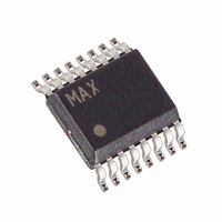
MAX8554EEE+ Maxim Integrated Products, MAX8554EEE+ Datasheet - Page 16

MAX8554EEE+
Manufacturer Part Number
MAX8554EEE+
Description
IC CNTRLR BUCK PWM 16-QSOP
Manufacturer
Maxim Integrated Products
Datasheet
1.MAX8553EEE.pdf
(24 pages)
Specifications of MAX8554EEE+
Pwm Type
Controller
Number Of Outputs
1
Frequency - Max
550kHz
Duty Cycle
95%
Voltage - Supply
4.5 V ~ 28 V
Buck
Yes
Boost
No
Flyback
No
Inverting
No
Doubler
No
Divider
Yes
Cuk
No
Isolated
No
Operating Temperature
-40°C ~ 85°C
Package / Case
16-QSOP
Frequency-max
550kHz
Output Voltage
0.6 V to 3.5 V
Output Current
25000 mA
Mounting Style
SMD/SMT
Switching Frequency
550 KHz
Maximum Operating Temperature
+ 85 C
Minimum Operating Temperature
- 40 C
Synchronous Pin
No
Topology
Buck
Dc
0649
Lead Free Status / RoHS Status
Lead free / RoHS Compliant
This algorithm results in a nearly constant switching fre-
quency despite the lack of a fixed-frequency clock
generator. The actual switching frequency, which is
given by the following equation, varies slightly due to
the voltage drop across the on-resistance of the
MOSFETs and the DC resistance of the output inductor:
where D is the duty cycle:
where I
tance of the low-side MOSFET, R
tance of the high-side MOSFET, and R
resistance of the output inductor. The ideal switching fre-
quency for V
quency increases for positive (sourcing) load current
and decreases for negative (sinking) load current, due to
the changing voltage drop across the low-side MOSFET,
which changes the inductor-current discharge ramp
rate. The on-times guaranteed in the Electrical
Characteristics are also influenced by switching delays
caused by the loading effect of the external power
MOSFETs.
The switching frequency can also be adjusted to a
value other than the preset frequencies by adding a
resistor voltage-divider at HSD. See the Adjusting the
Switching Frequency section.
4.5V to 28V Input, Synchronous PWM Buck Controllers
for DDR Termination and Point-of-Load Applications
Table
Table
16
FSEL CONNECTED TO
FSEL CONNECTED TO
______________________________________________________________________________________
O
Floating
Floating
Ground
Ground
1. Configuration of FSEL (MAX8553)
2. Configuration of FSEL (MAX8554)
REF
REF
is the output current, R
VL
D
VL
REFIN
=
V
f
HSD
S
V
= 2.5V is about 550kHz. Switching fre-
OUT
=
+
t
I R
O
ON
+
D
(
I R
O
DSONL
(
≅
DSONL
K
1.07
1.33
2.00
3.00
1.07
1.33
2.00
3.00
DSONH
DSONL
N
N
×
1
-
N
R
+
DSONH
R
DC
is the on-resis-
is the on-resis-
DC
)
)
is the DC
t
t
ON
ON
0.91
1.15
1.70
2.55
0.37
0.49
0.71
1.02
(µs)
(µs)
The MAX8553’s VTTR output is capable of sourcing or
sinking up to 25mA of current. The VTTR output voltage
is one-half of the voltage applied to REFIN. Bypass
VTTR with at least a 1µF ceramic capacitor.
The voltage at REF is nominally 2.00V. Connect a 0.22µF
ceramic bypass capacitor between REF and GND.
EN is a logic input used to enable or shut down the
MAX8554. Drive EN high or connect to V+ to enable the
output. Drive EN low to place the MAX8554 in low-
power shutdown mode, reducing input current to less
than 5µA (typ).
HSD senses the input voltage at the drain of the high-side
MOSFET, which is used to set the high-side MOSFET on-
time. For normal operation, connect HSD to the drain of
the high-side MOSFET.
In order to reduce pin count and package size, the
MAX8553 features a dual-function input pin, EN/HSD.
When EN/HSD is pulled to ground, the internal circuitry
powers off, reducing current consumption to less than
5µA (typ). To enable normal operation, connect
EN/HSD to the drain of the high-side MOSFET through
a 5.1kΩ resistor
becomes an input that monitors the high-side MOSFET
drain voltage (converter input voltage) and uses that
measurement to calculate the appropriate on-time for the
converter. If the enable function is not used, connect
EN/HSD directly to the high-side MOSFET drain.
FREQUENCY (kHz)
FREQUENCY (kHz)
EN/HSD Function (MAX8553 Only)
VTTR Reference (MAX8553 Only)
(Figure
550
400
300
200
550
400
300
200
EN and HSD (MAX8554 Only)
2). In this configuration, EN/HSD
Voltage Reference
V
V
V
V
HSD
HSD
HSD
HSD
V
V
V
V
OUT
OUT
OUT
OUT
= 12V, V
= 12V, V
= 12V, V
= 12V, V
CONDITION
CONDITION
/ V
/ V
/ V
/ V
EN/HSD
EN/HSD
EN/HSD
EN/HSD
OUT
OUT
OUT
OUT
= 0.5
= 0.5
= 0.5
= 0.5
= 2.5V
= 2.5V
= 2.5V
= 2.5V


