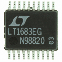
LTC1922EG-1 Linear Technology, LTC1922EG-1 Datasheet - Page 20

LTC1922EG-1
Manufacturer Part Number
LTC1922EG-1
Description
IC CTRLR PWM SYNC 20SSOP
Manufacturer
Linear Technology
Datasheet
1.LTC1922EG-1PBF.pdf
(24 pages)
Specifications of LTC1922EG-1
Pwm Type
Voltage/Current Mode
Number Of Outputs
1
Frequency - Max
1MHz
Duty Cycle
99%
Buck
No
Boost
No
Flyback
No
Inverting
No
Doubler
No
Divider
No
Cuk
No
Isolated
Yes
Operating Temperature
-40°C ~ 85°C
Package / Case
20-SSOP
Frequency-max
1MHz
Lead Free Status / RoHS Status
Contains lead / RoHS non-compliant
Voltage - Supply
-
Available stocks
Company
Part Number
Manufacturer
Quantity
Price
Company:
Part Number:
LTC1922EG-1
Manufacturer:
IBM
Quantity:
942
Part Number:
LTC1922EG-1
Manufacturer:
LT
Quantity:
20 000
OPERATIO
LTC1922-1
snubber capacitor and/or a very low resistance turn-off
driver. If synchronous rectifier MOSFETs are used on the
secondary, the same general guidelines apply. Keep in
mind, however, that the BV
be greater than V
secondary is snubbed. Without snubbing, the secondary
voltage can ring to levels far beyond what is expected due
to the resonant tank circuit formed between the secondary
leakage inductance and the C
the synchronous rectifier MOSFETs.
Switching Frequency Selection
Unless constrained by other system requirements, the
power converter’s switching frequency is usually set as
high as possible while staying within the desired efficiency
target. The benefits of higher switching frequencies are
many including smaller size, weight and reduced bulk
capacitance. In the full-bridge phase shift converter, these
principles are generally the same with the added compli-
cation of maintaining zero voltage transitions, and there-
fore, higher efficiency. ZVS is achieved in a finite time
during the switching cycle. During the ZVS time, power is
not delivered to the output; the act of ZVS reduces the
maximum available duty cycle. This reduction is propor-
tional to maximum output power since the parasitic ca-
pacitive element (MOSFETs) that increase ZVS time get
larger as power levels increase. This implies an inverse
relationship between output power level and switching
frequency. Table 1 displays recommended maximum
switching frequency vs power level for a 30V/75V in to
3.3V/5V out converter. Higher switching frequencies can
be used if the input voltage range is limited, the output
voltage is lower and/or lower efficiency can be tolerated.
Table 1.Switching Frequency vs Power Level
20
<100W
<200W
<500W
<50W
<1kW
<2kW
U
IN(MAX)
/N, depending on how well the
DSS
OSS
rating needed for these can
(output capacitance) of
600kHz
450kHz
300kHz
200kHz
150kHz
100kHz
Closing the Feedback Loop
Closing the feedback loop with the full-bridge converter
involves identifying where the power stage and other
system poles/zeroes are located and then designing a
compensation network around the converters error ampli-
fier to shape the frequency response to insure adequate
phase margin and transient response. Additional modifi-
cations will sometimes be required in order to deal with
parasitic elements within the converter that can alter the
feedback response. The compensation network will vary
depending on the load current range and the type of output
capacitors used. In isolated applications, the compensa-
tion network is generally located on the secondary side of
the power supply, around the error amplifier of the
optocoupler driver, usually an LT1431or equivalent. In
nonisolated systems, the compensation network is lo-
cated around the LTC1922-1’s error amplifier.
In current mode control, the dominant system pole is
determined by the load resistance (V
capacitor 1/(2 • R
1/(2 • ESR • C
load regulation can be obtained if there is high loop gain at
DC. This requires an integrator type of compensator
around the error amplifier. A procedure is provided for
deriving the required compensation components. More
complex types of compensation networks can be used to
obtain higher bandwidth if necessary.
Step 1. Calculate location of minimum and maximum
output pole:
Step 2. Calculate ESR zero location:
Step 3. Calculate the feedback divider gain:
If Polymer electrolytic output capacitors are used, the ESR
zero can be employed in the overall loop compensation
and optimum bandwidth can be achieved. If aluminum
electrolytics are used, the loop will need to be rolled off
prior to the ESR zero frequency, making the loop response
F
F
F
R
P1(MIN)
P1(MAX)
Z1
B
/(R
= 1/(2 • R
B
+ R
= 1/(2 • R
= 1/(2 • R
T
) or V
O
) introduces a zero. Excellent DC line and
ESR
O
REF
• C
• C
O(MAX)
O(MIN)
/V
O
O
)
OUT
). The output capacitors ESR
• C
• C
O
O
)
)
O
/I
O
) and the output


