LT3574IMS#PBF Linear Technology, LT3574IMS#PBF Datasheet - Page 12

LT3574IMS#PBF
Manufacturer Part Number
LT3574IMS#PBF
Description
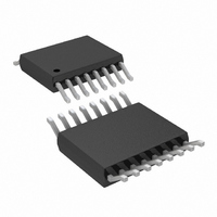
IC PWM FLYBCK ISO CM 16MSOP
Manufacturer
Linear Technology
Type
Flyback, Isolated, PWM - Current Moder
Datasheet
1.LT3574EMSPBF.pdf
(24 pages)
Specifications of LT3574IMS#PBF
Internal Switch(s)
Yes
Synchronous Rectifier
No
Number Of Outputs
1
Voltage - Output
Adj to 60V
Current - Output
650mA
Frequency - Switching
40kHz ~ 1MHz
Voltage - Input
3 ~ 40 V
Operating Temperature
-40°C ~ 125°C
Mounting Type
*
Package / Case
16-MSOP
Voltage - Supply
3 V ~ 40 V
Frequency-max
1MHz
Duty Cycle
52%
Pwm Type
Current Mode
Buck
No
Boost
No
Flyback
Yes
Inverting
No
Doubler
No
Divider
No
Cuk
No
Isolated
Yes
Lead Free Status / RoHS Status
Lead free / RoHS Compliant
Available stocks
Company
Part Number
Manufacturer
Quantity
Price
LT3574
Turns Ratio
Note that when using an R
output voltage, the user has relative freedom in selecting
a transformer turns ratio to suit a given application. In
contrast, simpler ratios of small integers, e.g., 1:1, 2:1,
3:2, etc., can be employed to provide more freedom in
setting total turns and mutual inductance.
Typically, the transformer turns ratio is chosen to maximize
available output power. For low output voltages (3.3V or 5V),
a N:1 turns ratio can be used with multiple primary windings
relative to the secondary to maximize the transformer’s
current gain (and output power). However, remember that
the SW pin sees a voltage that is equal to the maximum
input supply voltage plus the output voltage multiplied by
the turns ratio. This quantity needs to remain below the
abs max rating of the SW pin to prevent breakdown of the
internal power switch. Together these conditions place an
upper limit on the turns ratio, N, for a given application.
Choose a turns ratio low enough to ensure:
For larger N:1 values, a transformer with a larger physical
size is needed to deliver additional current and provide a
large enough inductance value to ensure that the off-time is
long enough to accurately measure the output voltage.
For lower output power levels, a 1:1 or 1:N transformer
can be chosen for the absolute smallest transformer size.
A 1:N transformer will minimize the magnetizing induc-
tance (and minimize size), but will also limit the available
output power. A higher 1:N turns ratio makes it possible
to have very high output voltages without exceeding the
breakdown voltage of the internal power switch.
applications inForMation
N
<
50 –
V
V V
OUT
IN MAX
+
(
V
F
)
FB
/R
REF
resistor ratio to set
Leakage Inductance
Transformer leakage inductance (on either the primary or
secondary) causes a voltage spike to appear at the primary
after the output switch turns off. This spike is increasingly
prominent at higher load currents where more stored
energy must be dissipated. In most cases, a snubber
circuit will be required to avoid overvoltage breakdown at
the output switch node. Transformer leakage inductance
should be minimized.
An RCD (resistor capacitor diode) clamp, shown in Fig-
ure 4, is required for most designs to prevent the leakage
inductance spike from exceeding the breakdown voltage
of the power device. The flyback waveform is depicted in
Figure 5. In most applications, there will be a very fast
voltage spike caused by a slow clamp diode that may not
exceed 60V. Once the diode clamps, the leakage inductance
current is absorbed by the clamp capacitor. This period
should not last longer than 150ns so as not to interfere
with the output regulation, and the voltage during this
clamp period must not exceed 55V. The clamp diode turns
off after the leakage inductance energy is absorbed and
the switch voltage is then equal to:
This voltage must not exceed 50V. This same equation
also determines the maximum turns ratio.
When choosing the snubber network diode, careful atten-
tion must be paid to maximum voltage seen by the SW
pin. Schottky diodes are typically the best choice to be
used in the snubber, but some PN diodes can be used if
they turn on fast enough to limit the leakage inductance
spike. The leakage spike must always be kept below 60V.
Figures 6 and 7 show the SW pin waveform for a 24V
5V
leakage spike is very high (more than 65V) with the bad
diode, while the good diode effectively limits the spike to
less than 55V.
V
OUT
SW(MAX)
application at a 0.5A load current. Notice that the
= V
IN(MAX)
+ N(V
OUT
+ V
F
)
3574f
IN
,


