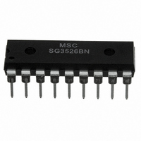
SG3526BN Microsemi Analog Mixed Signal Group, SG3526BN Datasheet - Page 7

SG3526BN
Manufacturer Part Number
SG3526BN
Description
IC PWM POWER SUPPLY SW 18DIP
Manufacturer
Microsemi Analog Mixed Signal Group
Datasheet
1.SG2526BN.pdf
(9 pages)
Specifications of SG3526BN
Pwm Type
Voltage Mode
Number Of Outputs
2
Frequency - Max
500kHz
Duty Cycle
49%
Voltage - Supply
8 V ~ 35 V
Buck
Yes
Boost
No
Flyback
No
Inverting
No
Doubler
No
Divider
No
Cuk
No
Isolated
No
Operating Temperature
0°C ~ 70°C
Package / Case
18-DIP
Frequency-max
500kHz
Lead Free Status / RoHS Status
Lead free / RoHS Compliant
Other names
SG3526BNR
SG3526BNR
SG3526BNR
Available stocks
Company
Part Number
Manufacturer
Quantity
Price
Rev 1.1a
Copyright
APPLICATION INFORMATION
DIGITAL CONTROL PORTS
The three digital control ports of the SG1526B are bi-
directional. Each pin can drive TTL and 5 volt CMOS logic
directly, up to a fan-out of 10 low-power Schottky gates.
Each pin can also be directly driven by open-collector TTL,
open-drain CMOS, and open-collector voltage comparators,
fan-in is equivalent to 1 low-power Schottky gate. Each port
is normally HIGH; the pin is pulled LOW to activate the
particular function. Driving SYNC LOW initiates a discharge
cycle in the oscillator. Pulling SHUTDOWN LOW immedi-
ately inhibits all PWM output pulses. Holding RESET LOW
discharges the soft-start capacitor. The logic threshold is
+1.1 volts at +25
expense of fan-out with an external 2K pull-up resistor to +5
volts.
OSCILLATOR
The oscillator is programmed for frequency and dead time
with three components: R
generated: a sawtooth waveform at pin 10 for pulse width
modulation, and a logic clock at pin 12. The following
procedure is recommended for choosing timing values:
The SG1526B can be synchronized to an external logic clock
by programming the oscillator to free-run at a frequency 10%
slower than the sync frequency. A periodic LOW logic pulse
approximately 0.5 Sec wide at the SYNC pin will then lock
the oscillator to the external frequency.
ERROR AMPLIFIER
The error amplifier is a transconductance design, with an
output impedance of 2 megohms. Since all voltage gain
takes place at the output pin, the open-loop gain/frequency
characteristics can be controlled with shunt reactance to
ground. When compensated for unity-gain stability with 100
pF, the amplifier has an open-loop pole at 400 Hz.
The input connections to the error amplifier and determined
by the polarity of the switching supply output voltage. For
positive supplies, the common-mode voltage is +5.0 volts
and the feedback connections in Figure 25A are used. With
negative supplies, the common-mode voltage is ground and
the feedback divider is connected between the negative
output and the +5.0 volt reference voltage, as shown in
Figure 25B.
1994
1. With R
2. If more dead time is required, select a larger value of
3. Increasing the dead time will cause the oscillator
for R
oscillator period. Remember that the frequency at
each driver output is half the oscillator frequency, and
the frequency at the +V
oscillator frequency.
R
increases by 300 ns/ .
frequency to decrease slightly. Go back and de-
crease the value of R
back to the nominal design value.
D
using Figure 14 as a guide. At 40 KHz dead time
T
D
and C
= 0 (pin 11 shorted to ground) select values
o
C. Noise immunity can be gained at the
T
from Figure 19 to give the desired
T
C
T
T
slightly to bring the frequency
, and R
C
terminal is the same as the
(continued)
D
. Two waveforms are
7
FIGURE 23
DIGITAL CONTROL PORT SCHEMATIC
Multiple devices can be synchronized together by program-
ming one master unit for the desired frequency, and then
sharing its sawtooth and clock waveforms with the slave
units. All C
master, and all SYNC terminals are likewise connected to
the SYNC pin of the master. Slave R
be left open; at least 50K should be connected from each pin
to ground. Slave R
grounded.
FIGURE 24.
OSCILLATOR CONNECTIONS ANDD WAVEFORMS
FIGURE 25.
ERROR AMPLIFIER CONNECTIONS
SG1526B/SG2526B/SG3526B
(A)
T
terminals are connected to the C
D
terminals may be either left open or
11861 Western Avenue
T
(714) 898-8121
terminals should not
(B)
Garden Grove, CA 92841
T
pin of the
FAX: (714) 893-2570


