ISL6420BIRZ-TK Intersil, ISL6420BIRZ-TK Datasheet
ISL6420BIRZ-TK
Specifications of ISL6420BIRZ-TK


Related parts for ISL6420BIRZ-TK

ISL6420BIRZ-TK Summary of contents
Page 1
... Externally Referenced Buck Converters CAUTION: These devices are sensitive to electrostatic discharge; follow proper IC Handling Procedures. | 1-888-INTERSIL or 1-888-468-3774 Intersil (and design registered trademark of Intersil Americas Inc. All other trademarks mentioned are the property of their respective owners. DS(ON) Copyright Intersil Americas Inc. 2009. All Rights Reserved ...
Page 2
... MARKING ISL6420BIAZ 6420B IAZ ISL6420BIAZ-TK (Note 1) 6420B IAZ ISL6420BIRZ 64 20BIRZ ISL6420BIRZ-TK (Note 1) 64 20BIRZ NOTES: 1. Please refer to TB347 for details on reel specifications. 2. These Intersil Pb-free plastic packaged products employ special Pb-free material sets, molding compounds/die attach materials, and 100% matte tin plate plus anneal (e3 termination finish, which is RoHS compliant and compatible with both SnPb and Pb-free soldering operations) ...
Page 3
Block Diagram REFOUT INTERNAL 0.6V GPIO1/REFIN SSDONE VOLTAGE GPIO2 MARGINING CONTROL VMSET/MODE CDEL FB COMP PGOOD PGOOD COMP VCC5 ENSS 10µA POWER-ON ENSS RESET (POR) SSDONE FAULT LOGIC PWM SS COMP V REF EA OSCILLATOR OV/UV COMP SGND RT VIN ...
Page 4
Typical 5V Input DC/DC Application Schematic 5V ±10 VIN ENSS RT PGOOD 0.1µF CDEL C 8 SGND Typical 5.5V to 28V Input DC/DC Application Schematic 5.5V to ...
Page 5
Typical 5V Input DC/DC Application Schematic 5V ±10 VIN ENSS RT CDEL PGOOD REF SGND CONFIGURATION FOR DDR TERMINATION/EXTERNALLY REFERENCED TRACKING APPLICATIONS Typical ...
Page 6
Typical 5V Input DC/DC Application Schematic 5V ±10 VIN ENSS RT PGOOD CDEL 0.1µ SGND Typical 5.5V to 28V Input DC/DC Application Schematic ...
Page 7
... Maximum Storage Temperature Range . . . -65°C to +150°C Ambient Temperature Range . -40°C to +85°C (for “I” suffix) Junction Temperature Range . . . . . . . . . . -40°C to +125°C Pb-Free Reflow Profile . . . . . . . . . . . . . . . . . .see link below http://www.intersil.com/pbfree/Pb-FreeReflow.asp TEST CONDITIONS ENSS = GND VIN = VCC5 for 5V configuration VIN = 5.6V to 28V, I ...
Page 8
Electrical Specifications Operating Conditions: VIN = 12V, PVCC shorted with VCC5, T apply over the operating temperature range, -40°C to +85°C. (Continued) PARAMETER SYMBOL Ramp Amplitude (Note 10) ΔV REFERENCE AND SOFT-START/ENABLE Internal Reference Voltage V Soft-Start Current Soft-Start Threshold ...
Page 9
Electrical Specifications Operating Conditions: VIN = 12V, PVCC shorted with VCC5, T apply over the operating temperature range, -40°C to +85°C. (Continued) PARAMETER SYMBOL Buffered Output Voltage - V REFOUT External Reference Buffered Output Voltage - V REFOUT External Reference ...
Page 10
Typical Performance Curves 0.604 0.602 0.600 0.598 0.596 0.594 -40 -15 10 TEMPERATURE (°C) FIGURE TEMPERATURE REF 1.15 1.05 0.95 0.85 -40 -15 10 TEMPERATURE (°C) FIGURE TEMPERATURE OCSET +25°C, VIN = 28V, I ...
Page 11
Typical Performance Curves FIGURE 7. EFFICIENCY vs LOAD CURRENT (V Pin Descriptions VIN This pin powers the controller and must be decoupled to ground using a ceramic capacitor as close as possible to the VIN pin. TABLE 1. INPUT SUPPLY ...
Page 12
CDEL The PGOOD signal can be delayed by a time proportional to a CDEL current of 2µA and the value of the capacitor connected between this pin and ground. A 0.1µF will typically provide 125ms delay. When in the Voltage ...
Page 13
TABLE 3. VOLTAGE MARGINING CONTROLLED BY GPIO1 AND GPIO2 GPIO1 GPIO2 Functional Description Initialization The ISL6420B automatically initializes upon receipt of power. The Power-On Reset (POR) function monitors the internal bias voltage ...
Page 14
The maximum r at the highest junction DS(ON) temperature. 2. Determine > I for OUT MAX where ΔI is the output inductor ripple current. A small ceramic capacitor should be placed in parallel with ...
Page 15
The slew time of the current is set by an external capacitor on the CDEL pin, which is charged and discharged with a 100µA current source. The change in voltage on the capacitor is 2.5V. This same capacitor is used ...
Page 16
V = 12V 3.3V at 25mA LOAD IN OUT FIGURE 14. PREBIASED OUTPUT AT 25mA LOAD Application Guidelines Layout Considerations As in any high frequency switching converter, layout is very important. Switching current from one power device to ...
Page 17
VIN OSC DRIVER PWM COMPARATOR DRIVER - + ΔV OSC E REFERENCE ERROR AMP DETAILED COMPENSATION COMPONENTS COMP ISL6420B REF ⎛ × ...
Page 18
The compensation gain uses external impedance networks Z and Z to provide a stable, high FB IN bandwidth (BW) overall loop. A stable control loop has a gain crossing with -20dB/decade slope and a phase margin greater than 45°. Include ...
Page 19
– RMS MAX For a through hole design, several electrolytic capacitors (Panasonic HFQ series or Nichicon PL series or Sanyo MV-GX ...
Page 20
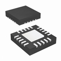
Package Outline Drawing L20.4x4 20 LEAD QUAD FLAT NO-LEAD PLASTIC PACKAGE Rev 1, 11/06 4.00 6 PIN 1 INDEX AREA 0.15 (4X) TOP VIEW ( 3. 6 TYP ) ( TYPICAL RECOMMENDED LAND PATTERN 20 ISL6420B 16X ...
Page 21
... Accordingly, the reader is cautioned to verify that data sheets are current before placing orders. Information furnished by Intersil is believed to be accurate and reliable. However, no responsibility is assumed by Intersil or its subsidiaries for its use; nor for any infringements of patents or other rights of third parties which may result from its use. No license is granted by implication or otherwise under any patent or patent rights of Intersil or its subsidiaries ...