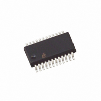
ISL6440IAZ-TK Intersil, ISL6440IAZ-TK Datasheet - Page 8

ISL6440IAZ-TK
Manufacturer Part Number
ISL6440IAZ-TK
Description
IC CTRLR PWM DUAL 300MHZ 24QSOP
Manufacturer
Intersil
Datasheet
1.ISL6440IAZ-T.pdf
(15 pages)
Specifications of ISL6440IAZ-TK
Pwm Type
Current Mode
Number Of Outputs
2
Frequency - Max
340kHz
Duty Cycle
93%
Voltage - Supply
4.5 V ~ 24 V
Buck
Yes
Boost
No
Flyback
No
Inverting
No
Doubler
No
Divider
No
Cuk
No
Isolated
No
Operating Temperature
-40°C ~ 85°C
Package / Case
24-QSOP
Frequency-max
340kHz
Lead Free Status / RoHS Status
Lead free / RoHS Compliant
Available stocks
Company
Part Number
Manufacturer
Quantity
Price
Company:
Part Number:
ISL6440IAZ-TK
Manufacturer:
Intersil
Quantity:
1 550
Part Number:
ISL6440IAZ-TK
Manufacturer:
INTERSIL
Quantity:
20 000
Pin Descriptions
BOOT2, BOOT1 - These pins power the upper MOSFET
drivers of each PWM converter. Connect this pin to the
junction of the bootstrap capacitor and the cathode of the
bootstrap diode. The anode of the bootstrap diode is
connected to the VCC_5V pin.
UGATE2, UGATE1 - These pins provide the gate drive for
the upper MOSFETs.
PHASE2, PHASE1 - These pins are connected to the junction
of the upper MOSFETs source, output filter inductor and lower
MOSFETs drain.
LGATE2, LGATE1 - These pins provide the gate drive for
the lower MOSFETs.
PGND - This pin provides the power ground connection for
the lower gate drivers for both PWM1 and PWM2. This pin
should be connected to the sources of the lower MOSFETs
and the (-) terminals of the external input capacitors.
FB2, FB1 - These pins are connected to the feedback
resistor divider and provide the voltage feedback signals for
the respective controller. They set the output voltage of the
converter. In addition, the PGOOD circuit uses these inputs
to monitor the output voltage status.
ISEN2, ISEN1 - These pins are used to monitor the voltage
drop across the lower MOSFET for current loop feedback
and overcurrent protection.
PGOOD - This is an open drain logic output used to indicate
the status of the output voltages. This pin is pulled low when
either of the two PWM outputs is not within 10% of the
respective nominal voltage.
SGND - This is the small-signal ground, common to both
controllers, and must be routed separately from the high
current ground (PGND). All voltage levels are measured with
respect to this pin. Connect the additional SGND pins to this
pin.
VIN - Use this pin to power the device with an external
supply voltage with a range of 5.6V to 24V. For 5V ±10%
operation, connect this pin to VCC5.
VCC5 - This pin is the output of the internal +5V linear
regulator. This output supplies the bias for the IC, the low
side gate drivers, and the external boot circuitry for the high
side gate drivers. The IC may be powered directly from a
single 5V (±10%) supply at this pin. When used as a 5V
supply input, this pin must be externally connected to V
The VCC5 pin must be always decoupled to power ground
with a recommended minimum of 4.7µF ceramic capacitor,
placed very close to the pin.
BIAS - This pin must be connected directly to VCC5.
SS1, SS2 - These pins provide a soft-start function for their
respective PWM controllers. When the chip is enabled, the
8
IN
.
ISL6440
regulated 5µA pull-up current source charges the capacitor
connected from this pin to ground. The error amplifier
reference voltage ramps from 0 to 0.8V while the voltage on
the soft-start pin ramps from 0 to 0.8V.
SD1, SD2 - These pins provide an enable/disable function
for their respective PWM output. The output is enabled when
this pin is floating or pulled HIGH, and disabled when the pin
is pulled LOW.
OCSET2, OCSET1 - A resistor from this pin to ground sets
the overcurrent threshold for the respective PWM.
Functional Description
General Description
The ISL6440 integrates control circuits for two synchronous
buck converters. The two synchronous bucks operate 180
degrees out of phase to substantially reduce the input ripple
and thus reduce the input filter requirements. The chip has
four control lines (SS1, SD1, SS2, and SD2), which provide
independent control for each of the synchronous buck
outputs.
The PWM controllers employ a free-running frequency of
300kHz. The current mode control scheme with an input
voltage feed-forward ramp input to the modulator provides
excellent rejection of input voltage variations and provides
simplified loop compensation.
Internal 5V Linear Regulator (VCC5)
All ISL6440 functions are internally powered from an on-
chip, low dropout, +5V regulator. The maximum regulator
input voltage is 24V. Bypass the regulator’s output (VCC5)
with a 4.7µF capacitor to ground. The dropout voltage for
this LDO is typically 600mV, so when VIN is greater then
5.6V, VCC5V is +5V. The ISL6440 also employs an
undervoltage lockout circuit that disables both regulators
when VCC5 falls below 4.4V.
The internal LDO can source over 60mA to supply the IC,
power the low side gate drivers, charge the external boot
capacitor and supply small external loads. When driving
large FETs, little or no regulator current may be available for
external loads.
For example, a single large FET with 30nC total gate charge
requires 30nC x 300kHz = 9mA. Thus four total FETs would
require 36mA. With 3mA for the internal bias would leave
approximately 20mA for an external +5V supply. Also, at
higher input voltages with larger FETs, the power dissipation
across the internal 5V will increase. Excessive dissipation
across this regulator must be avoided to prevent junction
temperature rise. Larger FETs can be used with 5V ±10%
input applications. The thermal overload protection circuit
will be triggered if the VCC5 output is short circuited.
Connect VCC5 to VIN for 5V ±10% input applications.
October 4, 2005
FN9040.2


