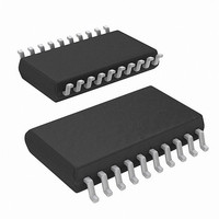
ISL6755AAZA-T Intersil, ISL6755AAZA-T Datasheet - Page 11

ISL6755AAZA-T
Manufacturer Part Number
ISL6755AAZA-T
Description
IC CTRLR PWM FULL-BRDG 20-QSOP
Manufacturer
Intersil
Datasheet
1.ISL6755AAZA.pdf
(17 pages)
Specifications of ISL6755AAZA-T
Pwm Type
Voltage/Current Mode
Number Of Outputs
4
Frequency - Max
2MHz
Duty Cycle
100%
Voltage - Supply
9 V ~ 16 V
Buck
No
Boost
No
Flyback
No
Inverting
No
Doubler
No
Divider
No
Cuk
No
Isolated
No
Operating Temperature
-40°C ~ 105°C
Package / Case
20-QSOP
Frequency-max
2MHz
Lead Free Status / RoHS Status
Lead free / RoHS Compliant
The peak overcurrent behavior is similar to most other PWM
controllers. If the peak current exceeds 1.0V, the active
output pulse is terminated immediately.
If voltage-mode control is used in a bridge topology, it should
be noted that peak current limit results in inherently unstable
operation. DC blocking capacitors used in voltage-mode
bridge topologies become unbalanced, as does the flux in
the transformer core. The average overcurrent circuitry
prevents this behavior by maintaining symmetric duty cycles
for each half-cycle. If the average current limit circuitry is not
used, a latching overcurrent shutdown method using
external components is recommended.
The CS to output propagation delay is increased by the
leading edge blanking (LEB) interval. The effective delay is
the sum of the two delays and is 130ns maximum.
Voltage Feed Forward Operation
Voltage feed forward is a technique used to regulate the
output voltage for changes in input voltage without the
intervention of the control loop. Voltage feed forward is often
implemented in voltage-mode control loops, but is redundant
and unnecessary in peak current-mode control loops.
Voltage feed forward operates by modulating the sawtooth
ramp in direct proportion to the input voltage. Figure 8
demonstrates the concept.
Input voltage feed forward may be implemented using the
RAMP input. An RC network connected between the input
voltage and ground, as shown in Figure 9, generates a
voltage ramp whose charging rate varies with the amplitude
of the source voltage. At the termination of the active output
pulse, RAMP is discharged to ground so that a repetitive
sawtooth waveform is created. The RAMP waveform is
compared to the VERR voltage to determine duty cycle. The
selection of the RC components depends upon the desired
input voltage operating range and the frequency of the
oscillator. In typical applications, the RC components are
ERROR VOLTAGE
FIGURE 8. VOLTAGE FEED FORWARD BEHAVIOR
OUTLL, LR
RAMP
VIN
CT
11
ISL6755
selected so that the ramp amplitude reaches 1.0V at
minimum input voltage within the duration of one half-cycle.
The charging time of the ramp capacitor is:
For optimum performance, the maximum value of the
capacitor should be limited to 10nF. The maximum DC
current through the resistor should be limited to 2mA
maximum. For example, if the oscillator frequency is
400kHz, the minimum input voltage is 300V, and a 4.7nF
ramp capacitor is selected, the value of the resistor can be
determined by rearranging Equation 9.
where t is equal to the oscillator period minus the deadtime.
If the deadtime is short relative to the oscillator period, it can
be ignored for this calculation.
If feed forward operation is not desired, the RC network may
be connected to VREF rather than the input voltage.
Alternatively, a resistor divider from CTBUF may be used as
the sawtooth signal. Regardless, a sawtooth waveform must
be generated on RAMP as it is required for proper PWM
operation.
Slope Compensation
Peak current-mode control requires slope compensation to
improve noise immunity, particularly at lighter loads, and to
prevent current loop instability, particularly for duty cycles
greater than 50%. Slope compensation may be
accomplished by summing an external ramp with the current
feedback signal or by subtracting the external ramp from the
R3
t
=
–
=
FIGURE 9. VOLTAGE FEED FORWARD CONTROL
R3 C7
-------------------------------------------------------------------------
C7
⋅
⋅
R3
C7
ln
⎛
⎜
⎝
⋅
1
ln
VIN
–
⎛
⎜
⎝
1
V
--------------------------------------- -
t –
RAMP PEAK
–
V
V
--------------------------------------- -
IN MIN )
RAMP PEAK
(
V
(
IN MIN
10
1
2
3
4
5
6
7
8
9
(
=
(
RAMP
)
159
)
)
⎞
⎟
⎠
ISL6755
=
)
⎞
⎟
⎠
------------------------------------------------------------
4.7 10
kΩ
GND
GND
⋅
S
–
20
19
16
15
14
13
12
11
2.5
18
17
–
9
⋅
⋅
ln
10
September 29, 2008
⎛
⎝
1
–
6
–
--------- -
300
1
FN6442.1
(EQ. 8)
⎞
⎠
(EQ. 9)


