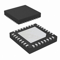
ISL9440BIRZ Intersil, ISL9440BIRZ Datasheet - Page 20

ISL9440BIRZ
Manufacturer Part Number
ISL9440BIRZ
Description
IC CTRLR PWM OUT-OF-PHASE 32-QFN
Manufacturer
Intersil
Datasheet
1.ISL9440BIRZ.pdf
(24 pages)
Specifications of ISL9440BIRZ
Pwm Type
Current Mode
Number Of Outputs
4
Frequency - Max
340kHz
Duty Cycle
93%
Voltage - Supply
4.5 V ~ 24 V
Buck
Yes
Boost
No
Flyback
No
Inverting
No
Doubler
No
Divider
No
Cuk
No
Isolated
No
Operating Temperature
-40°C ~ 85°C
Package / Case
32-VQFN Exposed Pad, 32-HVQFN, 32-SQFN, 32-DHVQFN
Frequency-max
340kHz
Lead Free Status / RoHS Status
Lead free / RoHS Compliant
Available stocks
Company
Part Number
Manufacturer
Quantity
Price
Part Number:
ISL9440BIRZ
Manufacturer:
INTERSIL
Quantity:
20 000
Company:
Part Number:
ISL9440BIRZ-T
Manufacturer:
Intersil
Quantity:
6 000
resistor depending on the maximum operating load current
and the value of the MOSFETs r
Choosing R
sample and hold circuitry is recommended, but values down
to 2µA and up to 100µA can be used. The higher sampling
current will help to stabilize the loop.
Due to the current loop feedback, the modulator has a single
pole response with -20dB slope at a frequency determined
by the load, as shown in Equation 8.
Where, R
For this type of modulator, a Type 2 compensation circuit is
usually sufficient.
Figure 42 shows a Type 2 amplifier and its response along
with the responses of the current mode modulator and the
converter. The Type 2 amplifier, in addition to the pole at
origin, has a zero-pole pair that causes a flat gain region at
frequencies in between the zero and the pole.
The zero frequency, the amplifier high-frequency gain, and
the modulator gain are chosen to satisfy most typical
applications. The crossover frequency will appear at the
point where the modulator attenuation equals the amplifier
high frequency gain. The only task that the system designer
has to complete is to specify the output filter capacitors to
position the load main pole somewhere within one decade
lower than the amplifier zero frequency. With this type of
F
F
F
R
Z
P
PO
MODULATOR
CS
G
=
=
M
≥
=
------------------------------ -
2π R
------------------------------ -
2π R
= 17.5dB
(
---------------------------------------------- -
FIGURE 42. FEEDBACK LOOP COMPENSATION
-------------------------------- -
2π R
I
MAX
⋅
⋅
O
EA
1
⋅
1
F
2
1
is load resistance and C
CONVERTER
CS
PO
30μA
) r
1
⋅
⋅
O
(
C
C
to provide 30µA of current to the current
⋅
DS ON
1
2
C
=
=
O
(
6kHz
600kHz
)
)
F
20
Z
DS(ON)
R1
F
O
C
G
is load capacitance.
EA
.
TYPE 2 EA
= 18dB
R2
C2
C1
F
ISL9440B, ISL9440C
P
(EQ. 10)
(EQ. 7)
(EQ. 8)
(EQ. 9)
compensation plenty of phase margin is easily achieved due
to zero-pole pair phase ‘boost’.
Conditional stability may occur only when the main load pole
is positioned too much to the left side on the frequency axis
due to excessive output filter capacitance. In this case, the
ESR zero placed within the 1.2kHz to 30kHz range gives
some additional phase ‘boost’. Some phase boost can also
be achieved by connecting capacitor C
upper resistor R
value. Please refer to “Output Capacitor Selection” on
page 22 and “Input Capacitor Selection” on page 23 for
further details.
Linear Regulator
The linear regulator controller is a trans-conductance
amplifier with a nominal gain of 2A/V. The N-Channel
MOSFET output buffer can sink a minimum of 50mA.
The reference voltage is 0.8V. With 0V differential at its
input, the controller sinks 21mA of current. For better load
regulation, it is recommended that the resistor from the LDO
input to the base of the PNP (or gate of the PFET) is set so
that the sink current at G4 pin is within 9mA to 31mA over
the entire load and temperature range.
An external PNP transistor or P-Channel MOSFET pass
device can be used. The dominant pole for the loop can be
placed at the base of the PNP (or gate of the PFET), as a
capacitor from emitter-to-base (source to gate of a PFET).
Better load transient response is achieved however, if the
dominant pole is placed at the output with a capacitor to
ground at the output of the regulator.
Under no-load conditions, leakage currents from the pass
transistors supply the output capacitors, even when the
transistor is off. Generally, this is not a problem since the
feedback resistor drains the excess charge. However,
charge may build up on the output capacitor making V
rise above its set point. Care must be taken to insure that the
feedback resistor’s current exceeds the pass transistors
leakage current over the entire temperature range.
60
50
40
30
20
10
0
0.79
FIGURE 43. LINEAR CONTROLLER GAIN
1
0.8
of the divider that sets the output voltage
FEEDBACK VOLTAGE (V)
0.81
0.82
Z
0.83
in parallel with the
0.84
June 24, 2010
FN6799.3
LDO
0.85


