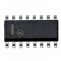
NCP1562BDR2G ON Semiconductor, NCP1562BDR2G Datasheet - Page 20

NCP1562BDR2G
Manufacturer Part Number
NCP1562BDR2G
Description
IC CLAMP/RESET PWM CTLR 16-SOIC
Manufacturer
ON Semiconductor
Datasheet
1.NCP1562ADBR2G.pdf
(26 pages)
Specifications of NCP1562BDR2G
Pwm Type
Voltage Mode
Number Of Outputs
2
Frequency - Max
1MHz
Duty Cycle
85%
Voltage - Supply
23.2 V ~ 100 V
Buck
No
Boost
Yes
Flyback
Yes
Inverting
Yes
Doubler
No
Divider
No
Cuk
No
Isolated
No
Operating Temperature
-40°C ~ 125°C
Package / Case
16-SOIC (3.9mm Width)
Frequency-max
1MHz
Topology
Flyback, Forward, Half-Bridge
Output Voltage
20 V
Output Current
2000 mA, 1000 mA
Switching Frequency
1000 KHz
Duty Cycle (max)
85 %
Maximum Operating Temperature
+ 125 C
Minimum Operating Temperature
- 40 C
Fall Time
10 ns
Mounting Style
SMD/SMT
Rise Time
26 ns
Synchronous Pin
Yes
Lead Free Status / RoHS Status
Lead free / RoHS Compliant
Other names
NCP1562BDR2G
NCP1562BDR2GOSTR
NCP1562BDR2GOSTR
Available stocks
Company
Part Number
Manufacturer
Quantity
Price
Company:
Part Number:
NCP1562BDR2G
Manufacturer:
ON Semiconductor
Quantity:
4 000
Part Number:
NCP1562BDR2G
Manufacturer:
ON/安森美
Quantity:
20 000
Ramp discharge current (I
(I
sharp FF Ramp transition. Equations 3 and 4 are used to
determine R
where, f is the operating frequency. It is recommended to
bias the FF circuit with enough current to provide good
noise immunity.
PWM Comparator
the duty cycle by comparing the error signal to the FF
Ramp. The error signal is fed into the V
can be driven directly with an optocoupler without the need
of an external pullup resistor as shown in Figure 45. In
some instances, it may be required to have a pullup resistor
smaller than the internal resistor (R4) to adjust the gain of
the isolation stage. This is easily accomplished by
connecting an external resistor (R
R
effective pullup resistance is the parallel combination of
R4 and R
incorporating a series diode and resistor. The series diode
provides a 0.7 V offset between the V
PWM Comparator inverting input. It allows reaching zero
duty cycle without the need of pulling the V
way to GND. The outputs are enabled if the V
approximately 0.5 V above the valley of the FF Ramp.
Outputs
adjustable overlap delay (t
a source resistance of 4.0 Ω (typ) and a sink resistance of
2.5 Ω (typ). The secondary output, OUT2, has a source and
a sink resistance of 12 Ω (typ). OUT1 is rated at a
maximum of 2.0 A and OUT2 is rated at a maximum of
Comparator
0.2 V
RFF
EA
The minimum value of R
In steady state operation, the PWM Comparator adjusts
The drive of the V
The NCP1562 has two in- - phase output drivers with an
PWM
) should be at least ten times smaller than I
is connected between the V
- -
+
+
- -
Figure 45. Optocoupler Driving V
EA
.
FF
270 kΩ
C FF =
and C
20 kΩ
2 kΩ
0.1 × I FF(D)
FF
ln
EA
.
V in
V in - -3 V
D
FF(D)
pin is simplified by internally
V in
V
FF
V
). The main output, OUT1, has
EA
REF
FF
). The current through R
FF Ramp
D
is determined by the FF
× f × R FF
R
≤ R FF
REF
EA
EA
) in parallel with R4.
(Optional)
EA
and V
EA
pin. The V
EA
input and the
EA
EA
Input
EA
3 V
0 V
FF(D)
pin all the
pins. The
voltage is
Feedback
Signal
http://onsemi.com
(eq. 3)
(eq. 4)
EA
for a
pin
FF
20
1.0 A. If a higher drive capability is required, an external
driver stage can be easily added as shown in Figure 46.
side P- - Channel active clamp MOSFET. A high side
N- - Channel active clamp MOSFET or a synchronous
rectifier can also be driven by inverting OUT2. OUT2 is
purposely sized smaller than OUT1 because the active
clamp MOSFET only sees the magnetizing current.
Therefore, a smaller active clamp MOSFET with less input
capacitance can be used compared to the main switch.
internal startup circuit is disabled and the outputs are
enabled if no faults are present. Otherwise, the outputs
remain disabled until the fault is removed and V
reaches V
sequence if V
7.0 V.
state voltage is approximately V
auxiliary supply voltage should not exceed the maximum
gate voltage of the main or active clamp MOSFET.
generate inductance- - induced spikes if inductance is not
reduced on the outputs. This can be done by reducing the
connection length between the drivers and their loads and
using wide connections.
Overlap Delay
the main and active clamp MOSFETs. The secondary
output, OUT2, precedes OUT1 during a low to high
transition and trails OUT1 during a high to low transition.
Figure 47 shows the relationship between OUT1 and
OUT2.
OUT1 drives the main MOSFET, and OUT2 drives a low
Once V
The outputs are biased directly from V
The high current drive capability of the outputs will
The overlap delay prevents simultaneous conduction of
Figure 46. Discrete Boost Drive Stage
AUX(on)
t
AUX
D
Figure 47. Output Timing Diagram
(Leading)
AUX
V
reaches V
OUT1
OUT2
AUX
. The outputs are disabled after a soft- - stop
OUT1
OUT2
or
is below V
AUX(on)
AUX(on)
Output
(typically 10.3 V), the
AUX
t
D
or if V
AUX
(Trailing)
. Therefore, the
and their high
AUX
reaches
AUX


