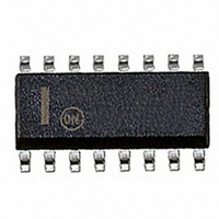
NCP1562BDR2G ON Semiconductor, NCP1562BDR2G Datasheet - Page 5

NCP1562BDR2G
Manufacturer Part Number
NCP1562BDR2G
Description
IC CLAMP/RESET PWM CTLR 16-SOIC
Manufacturer
ON Semiconductor
Datasheet
1.NCP1562ADBR2G.pdf
(26 pages)
Specifications of NCP1562BDR2G
Pwm Type
Voltage Mode
Number Of Outputs
2
Frequency - Max
1MHz
Duty Cycle
85%
Voltage - Supply
23.2 V ~ 100 V
Buck
No
Boost
Yes
Flyback
Yes
Inverting
Yes
Doubler
No
Divider
No
Cuk
No
Isolated
No
Operating Temperature
-40°C ~ 125°C
Package / Case
16-SOIC (3.9mm Width)
Frequency-max
1MHz
Topology
Flyback, Forward, Half-Bridge
Output Voltage
20 V
Output Current
2000 mA, 1000 mA
Switching Frequency
1000 KHz
Duty Cycle (max)
85 %
Maximum Operating Temperature
+ 125 C
Minimum Operating Temperature
- 40 C
Fall Time
10 ns
Mounting Style
SMD/SMT
Rise Time
26 ns
Synchronous Pin
Yes
Lead Free Status / RoHS Status
Lead free / RoHS Compliant
Other names
NCP1562BDR2G
NCP1562BDR2GOSTR
NCP1562BDR2GOSTR
Available stocks
Company
Part Number
Manufacturer
Quantity
Price
Company:
Part Number:
NCP1562BDR2G
Manufacturer:
ON Semiconductor
Quantity:
4 000
Part Number:
NCP1562BDR2G
Manufacturer:
ON/安森美
Quantity:
20 000
Stresses exceeding Maximum Ratings may damage the device. Maximum Ratings are stress ratings only. Functional operation above the
Recommended Operating Conditions is not implied. Extended exposure to stresses above the Recommended Operating Conditions may affect
device reliability.
1. This device series contains ESD protection and exceeds the following tests:
2. This device contains Latchup protection and exceeds 100 mA per JEDEC Standard JESD78.
MAXIMUM RATINGS
Line Voltage
Auxiliary Supply, OUT1, OUT2
All Other Inputs/Outputs Voltage
All Other Inputs/Outputs Current
5.0 V Reference Output Current
5.0 V Reference Output Voltage
OUT1 Peak Output Current (D = 2%)
OUT2 Peak Output Current (D = 2%)
Operating Junction Temperature
Storage Temperature Range
Power Dissipation (T
Thermal Resistance, Junction to Ambient (2.0 Oz Cu Printed Circuit Copper Clad)
Pin 1 is the HV startup of the device and is rated to the max rating of the part, or 100 V.
DT Suffix, Plastic Package Case 948F (TSSOP- -16)
D Suffix, Plastic Package Case 751B (SO- -16)
DT Suffix, Plastic Package Case 948F (TSSOP- -16)
D Suffix, Plastic Package Case 751B (SO- -16)
Pins 2- -16:
0.36 Sq In
1.0 Sq In
0.36 Sq In
1.0 Sq In
A
= 25_C, 2.0 Oz Cu, 1.0 Sq Inch Printed Circuit Copper Clad)
(Notes 1 and 2)
Human Body Model 2000 V per MIL–STD–883, Method 3015.
Machine Model Method 160 V.
Rating
http://onsemi.com
5
V
AUX
Symbol
V
R
I
I
I
T
V
V
REF
out1
out2
I
P
T
REF
θJA
IO
stg
, V
IO
in
J
D
outx
–40 to +125
–55 to +150
- -0.3 to 6.0
Value
0.75
0.95
100
155
133
120
105
5.0
2.5
1.0
20
10
10
_C/W
Unit
mA
mA
_C
_C
W
V
V
V
V
A
A


