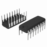
CS4124YN16 ON Semiconductor, CS4124YN16 Datasheet

CS4124YN16
Specifications of CS4124YN16
Available stocks
Related parts for CS4124YN16
CS4124YN16 Summary of contents
Page 1
... PIN CONNECTION AND MARKING DIAGRAM 1 OUTPUT BOOST FLT R OSC C OSC CTL PGND Assembly Location WL Wafer Lot YY Year WW Work Week ORDERING INFORMATION* Device Package CS4124YN16 DIP– GND INH I ADJ I SENSE+ I SENSE– PMP SNI V REG Shipping 25 Units/Rail Publication Order Number: CS4124/D ...
Page 2
V 42.5 H BAT 1000 F 1000 100 F PWM Input ABSOLUTE MAXIMUM RATINGS* Storage Temperature Range Peak Transient Voltage (load dump = 26 V ...
Page 3
ELECTRICAL CHARACTERISTICS Characteristic V Supply CC Operating Current Supply Quiescent Current Overvoltage Shutdown Control (CTL) Control Input Current Sleep Mode Threshold Sleep Mode Hysteresis Control Sense Differential Voltage Sense I Input Current ADJ Linear Regulator Output Voltage, V REG Inhibit ...
Page 4
ELECTRICAL CHARACTERISTICS (continued) Characteristic External Drive (OUTPUT) (continued) Output Sink Current Output Source Current Output High Voltage Output Low Voltage Charge Pump (DRV) Boost Voltage PIN FUNCTION DESCRIPTION PACKAGE PIN # 16 Lead PDIP ...
Page 5
GND V 5.0 V Regulator REG Overvoltage Clamp V CC PGND CTL Oscillator C OSC CS4124 450 Reset Triangle Timer Out In R FLT OSC Figure 2. Block Diagram http://onsemi.com 5 PMP SNI ...
Page 6
TYPICAL PERFORMANCE CHARACTERISTICS 5. 4.96 4.94 – Temperature Figure 3. V vs. Temperature @ I REG 1.3 1.2 1.1 I ...
Page 7
... Voltage Duty Cycle Conversion The IC translates an input voltage at the CTL lead into a duty cycle at the OUTPUT lead. The transfer function incorporates ON Semiconductor’s patented Voltage Compensation method to keep the average voltage and current across the load constant regardless of fluctuations in the supply voltage. The duty cycle is varied based upon the input voltage and supply voltage by the following equation: 2 ...
Page 8
IC reverts back to run mode until another fault occurs number of faults occur in a given period of time, the IC “times out” and disables the MOSFET for a long period of time to ...
Page 9
PACKAGE DIMENSIONS –A– –T– PACKAGE THERMAL DATA Parameter CS4124 DIP–16 N SUFFIX CASE 648–08 ISSUE DIP–16 Typical 42 Typical 80 http://onsemi.com 9 ...
Page 10
Notes CS4124 http://onsemi.com 10 ...
Page 11
Notes CS4124 http://onsemi.com 11 ...
Page 12
... CENTRAL/SOUTH AMERICA: Spanish Phone: 303–308–7143 (Mon–Fri 8:00am to 5:00pm MST) Email: ONlit–spanish@hibbertco.com ASIA/PACIFIC: LDC for ON Semiconductor – Asia Support Phone: 303–675–2121 (Tue–Fri 9:00am to 1:00pm, Hong Kong Time) Toll Free from Hong Kong & Singapore: 001–800–4422–3781 Email: ONlit– ...


