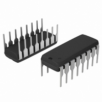
CS4124YN16 ON Semiconductor, CS4124YN16 Datasheet - Page 7

CS4124YN16
Manufacturer Part Number
CS4124YN16
Description
IC CTRLR PWM FET HI SIDE 16DIP
Manufacturer
ON Semiconductor
Datasheet
1.CS4124YN16.pdf
(12 pages)
Specifications of CS4124YN16
Pwm Type
Controller
Number Of Outputs
1
Frequency - Max
25kHz
Duty Cycle
100%
Voltage - Supply
4 V ~ 26 V
Buck
No
Boost
Yes
Flyback
No
Inverting
No
Doubler
No
Divider
No
Cuk
No
Isolated
No
Operating Temperature
-40°C ~ 125°C
Package / Case
16-DIP (0.300", 7.62mm)
Frequency-max
25kHz
Lead Free Status / RoHS Status
Contains lead / RoHS non-compliant
Other names
CS4124YN16OS
Available stocks
Company
Part Number
Manufacturer
Quantity
Price
Company:
Part Number:
CS4124YN16
Manufacturer:
MOTOROLA
Quantity:
9
Company:
Part Number:
CS4124YN16
Manufacturer:
ON Semiconductor
Quantity:
48
Oscillator
C
components R
to V
function properly. In order to keep the frequency of the
oscillator constant the current that charges C
vary with supply. R
C
therefore:
C
frequencies over the range of 15 Hz to 25 kHz. With the
suggested values of 93.1 k and 470 pF for R
the nominal frequency will be approximately 20 kHz.
I
change over a more than 2:1 ratio and therefore C
be changed to adjust the oscillator frequency.
Voltage Duty Cycle Conversion
duty cycle at the OUTPUT lead. The transfer function
incorporates ON Semiconductor’s patented Voltage
Compensation method to keep the average voltage and
current across the load constant regardless of fluctuations in
the supply voltage. The duty cycle is varied based upon the
input voltage and supply voltage by the following equation:
is compared to the oscillator voltage to produce the
compensated duty cycle. The transfer is set up so that when
V
For example at V
the duty cycle would be 50% at the output. This would place
ROSC
OSC
OSC
OSC
CC
The IC sets up a constant frequency triangle wave at the
The peak and valley of the triangle wave are proportional
This is required to make the voltage compensation
I
The period of the oscillator is:
The R
The IC translates an input voltage at the CTL lead into a
An internal DC voltage equal to:
ROSC
CC
= 14 V the duty cycle will equal V
. The voltage across R
, at V
lead. Therefore:
lead whose frequency is related to the external
by the following:
OSC
is multiplied by (2) internally and transferred to the
V DC + (1.683
T + 2C OSC
Duty Cycle + 100%
CC
and C
Frequency +
OSC
= 14 V, will be 66.7 A. I
THEORY OF OPERATION
CC
V VALLEY + 0.1
I ROSC + 0.5
V PEAK + 0.7
and C
OSC
I COSC +"
= 14 V, V
OSC
components can be varied to create
OSC
sets up the current which charges
V PEAK * V VALLEY
R OSC
V CTL ) ) V VALLEY
, by the following equation:
REG
OSC
R OSC
V CC
= 5.0 V and V
I COSC
0.83
R OSC
2.8
V CC
V CC
is 50% of V
V CC
CTL
C OSC
V CC
V CTL
divided by V
ROSC
APPLICATIONS INFORMATION
OSC
OSC
CTL
OSC
should not
and C
must also
CC
= 2.5 V,
http://onsemi.com
should
OSC
REG
and
CS4124
,
.
7
a 7.0 V average voltage across the load. If V
to 10 V, the IC would change the duty cycle to 70% and
hence keep the average load voltage at 7.0 V.
5.0 V Linear Regulator
V
for many internal and external functions. It has a drop out of
approximately 1.5 V at room temperature.
Current Sense and Timer
by cycle basis at the I
differential voltage across these two leads is amplified
internally and compared to the voltage at the I
gain, A
equation:
resistor (R
terminals and the voltage at the I
low pass filter which filters out high frequency noise
generated by the switching of the external MOSFET and the
associated lead noise. R
gain of the I
leads are low impedance inputs thereby creating a good
current sensing amplifier. Both leads source 50 A while the
chip is in run mode. I
4.0 V. When the current through the external MOSFET
exceeds I
gate of the MOSFET low for the remainder of the oscillator
cycle (fault mode). At the start of the next cycle, the latch is
REG
120
There is a 5.0 V, 5.0 mA linear regulator available at the
The IC differentially monitors the load current on a cycle
The current limit (I
The R
100
60
20
40
80
0
10
A V +
lead for external use. This voltage acts as a reference
V
CS
LIM
is set internally and externally by the following
SENSE
resistors and C
20
I SENSE) * I SENSE *
Figure 7. Voltage Compensation
LIM
I LIM +
, an internal latch is set and the output pulls the
equation because the I
) placed across the I
30
ADJ
CTL Voltage (% of V
V I(ADJ)
1000 ) R CS
LIM
40
37000
CS
should be biased between 1.0 V and
) is set by the external current sense
SENSE+
CS
V
also forms an error term in the
CC
components form a differential
50
V
CC
= 14 V
ADJ
= 8.0 V
and I
V
60
CC
R SENSE
lead.
V I(ADJ)
+
= 16 V
SENSE+
REG
SENSE+
SENSE–
70
1000 ) R CS
)
37000
CC
ADJ
80
and I
and I
leads. The
then drops
lead. The
90
SENSE–
SENSE–
100


